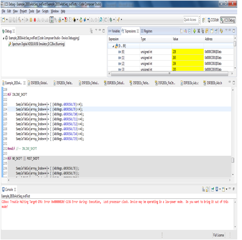
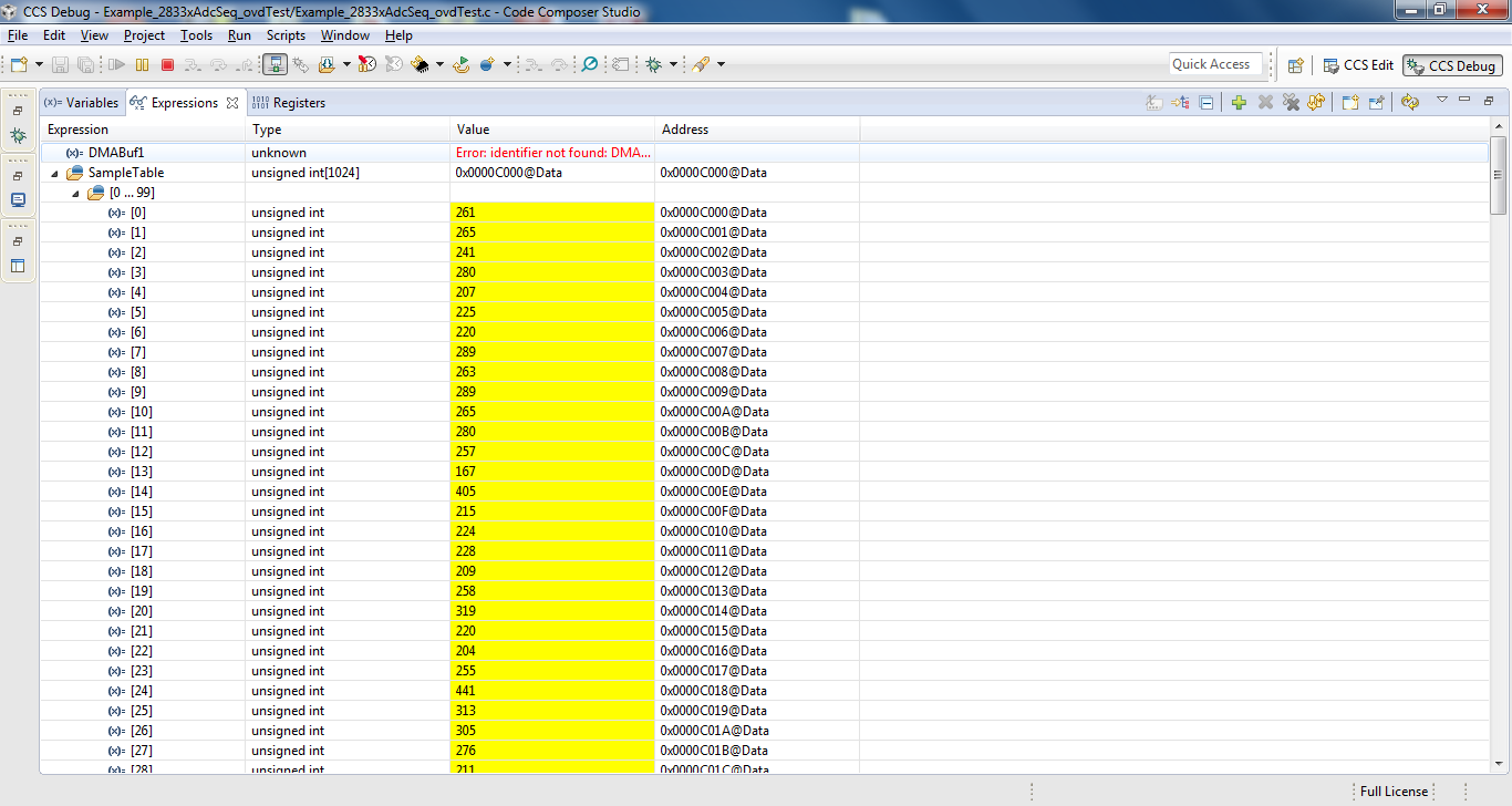
Q.1. In the below mentioned code when I am using the "sampleTable" in watch variable window the value of the expression "sampleTable" are not giving the maximum value i.e. 4096.So What is the reason behind this fault ?
Q.2.How is the program working?
// Watch Variables:
// SampleTable - Log of converted values.
// GPIO34 - Toggles on every ADC sequencer flag
//
//###########################################################################
//
// Original source by: S.S.
//
// $TI Release: DSP2833x/DSP2823x C/C++ Header Files V1.31 $
// $Release Date: August 4, 2009 $
//###########################################################################
#include "DSP28x_Project.h" // Device Headerfile and Examples Include File
// Determine when the shift to right justify the data takes place
// Only one of these should be defined as 1.
// The other two should be defined as 0.
#define POST_SHIFT 0 // Shift results after the entire sample table is full
#define INLINE_SHIFT 1 // Shift results as the data is taken from the results regsiter
#define NO_SHIFT 0 // Do not shift the results
// ADC start parameters
#if (CPU_FRQ_150MHZ) // Default - 150 MHz SYSCLKOUT
#define ADC_MODCLK 0x3 // HSPCLK = SYSCLKOUT/2*ADC_MODCLK2 = 150/(2*3) = 25.0 MHz
#endif
#if (CPU_FRQ_100MHZ)
#define ADC_MODCLK 0x2 // HSPCLK = SYSCLKOUT/2*ADC_MODCLK2 = 100/(2*2) = 25.0 MHz
#endif
#define ADC_CKPS 0x0 // ADC module clock = HSPCLK/1 = 25.5MHz/(1) = 25.0 MHz
#define ADC_SHCLK 0x1 // S/H width in ADC module periods = 2 ADC cycle
#define AVG 1000 // Average sample limit
#define ZOFFSET 0x00 // Average Zero offset
#define BUF_SIZE 1024 // Sample buffer size
// Global variable for this example
Uint16 SampleTable[BUF_SIZE];
main()
{
Uint16 i;
Uint16 array_index;
// Step 1. Initialize System Control:
// PLL, WatchDog, enable Peripheral Clocks
// This example function is found in the DSP2833x_SysCtrl.c file.
InitSysCtrl();
// Specific clock setting for this example:
EALLOW;
SysCtrlRegs.HISPCP.all = ADC_MODCLK; // HSPCLK = SYSCLKOUT/ADC_MODCLK
EDIS;
// Step 2. Initialize GPIO:
// This example function is found in the DSP2833x_Gpio.c file and
// illustrates how to set the GPIO to it's default state.
// InitGpio(); // Skipped for this example
// Enable the pin GPIO34 as output
EALLOW;
GpioCtrlRegs.GPBMUX1.bit.GPIO34 = 0; // GPIO pin
GpioCtrlRegs.GPBDIR.bit.GPIO34 = 1; // Output pin
EDIS;
// Step 3. Clear all interrupts and initialize PIE vector table:
// Disable CPU interrupts
DINT;
// Initialize the PIE control registers to their default state.
// The default state is all PIE interrupts disabled and flags
// are cleared.
// This function is found in the DSP2833x_PieCtrl.c file.
InitPieCtrl();
// Disable CPU interrupts and clear all CPU interrupt flags:
IER = 0x0000;
IFR = 0x0000;
// Initialize the PIE vector table with pointers to the shell Interrupt
// Service Routines (ISR).
// This will populate the entire table, even if the interrupt
// is not used in this example. This is useful for debug purposes.
// The shell ISR routines are found in DSP2833x_DefaultIsr.c.
// This function is found in DSP2833x_PieVect.c.
InitPieVectTable();
// Step 4. Initialize all the Device Peripherals:
// This function is found in DSP2833x_InitPeripherals.c
// InitPeripherals(); // Not required for this example
InitAdc(); // For this example, init the ADC
// Specific ADC setup for this example:
AdcRegs.ADCTRL1.bit.ACQ_PS = ADC_SHCLK; // Sequential mode: Sample rate = 1/[(2+ACQ_PS)*ADC clock in ns]
// = 1/(3*40ns) =8.3MHz (for 150 MHz SYSCLKOUT)
// = 1/(3*80ns) =4.17MHz (for 100 MHz SYSCLKOUT)
// If Simultaneous mode enabled: Sample rate = 1/[(3+ACQ_PS)*ADC clock in ns]
AdcRegs.ADCTRL3.bit.ADCCLKPS = ADC_CKPS;
AdcRegs.ADCTRL1.bit.SEQ_CASC = 1; // 1 Cascaded mode
AdcRegs.ADCCHSELSEQ1.bit.CONV00 = 0x0;
AdcRegs.ADCTRL1.bit.CONT_RUN = 1; // Setup continuous run
AdcRegs.ADCTRL1.bit.SEQ_OVRD = 1; // Enable Sequencer override feature
AdcRegs.ADCCHSELSEQ1.all = 0x0; // Initialize all ADC channel selects to A0
AdcRegs.ADCCHSELSEQ2.all = 0x0;
AdcRegs.ADCCHSELSEQ3.all = 0x0;
AdcRegs.ADCCHSELSEQ4.all = 0x0;
AdcRegs.ADCMAXCONV.bit.MAX_CONV1 = 0x7; // convert and store in 8 results registers
// Step 5. User specific code, enable interrupts:
// Clear SampleTable
for (i=0; i<BUF_SIZE; i++)
{
SampleTable[i] = 0;
}
// Start SEQ1
AdcRegs.ADCTRL2.all = 0x1999;
for(;;)
{ // Take ADC data and log them in SampleTable array
// Initalize the array index. This points to the current
// location within the SampleTable
array_index = 0;
for (i=0; i<(BUF_SIZE/16); i++)
{
// Wait for int1
while (AdcRegs.ADCST.bit.INT_SEQ1== 0){}
GpioDataRegs.GPBSET.bit.GPIO34 = 1; // Set GPIO34 for monitoring -optional
AdcRegs.ADCST.bit.INT_SEQ1_CLR = 1;
#if INLINE_SHIFT
SampleTable[array_index++]= ( (AdcRegs.ADCRESULT0)>>4);
SampleTable[array_index++]= ( (AdcRegs.ADCRESULT1)>>4);
SampleTable[array_index++]= ( (AdcRegs.ADCRESULT2)>>4);
SampleTable[array_index++]= ( (AdcRegs.ADCRESULT3)>>4);
SampleTable[array_index++]= ( (AdcRegs.ADCRESULT4)>>4);
SampleTable[array_index++]= ( (AdcRegs.ADCRESULT5)>>4);
SampleTable[array_index++]= ( (AdcRegs.ADCRESULT6)>>4);
SampleTable[array_index++]= ( (AdcRegs.ADCRESULT7)>>4);
#endif //-- INLINE_SHIFT
#if NO_SHIFT || POST_SHIFT
SampleTable[array_index++]= ( (AdcRegs.ADCRESULT0));
SampleTable[array_index++]= ( (AdcRegs.ADCRESULT1));
SampleTable[array_index++]= ( (AdcRegs.ADCRESULT2));
SampleTable[array_index++]= ( (AdcRegs.ADCRESULT3));
SampleTable[array_index++]= ( (AdcRegs.ADCRESULT4));
SampleTable[array_index++]= ( (AdcRegs.ADCRESULT5));
SampleTable[array_index++]= ( (AdcRegs.ADCRESULT6));
SampleTable[array_index++]= ( (AdcRegs.ADCRESULT7));
#endif //-- NO_SHIFT || POST_SHIFT
while (AdcRegs.ADCST.bit.INT_SEQ1== 0){}
GpioDataRegs.GPBCLEAR.bit.GPIO34 = 1; // Clear GPIO34 for monitoring -optional
AdcRegs.ADCST.bit.INT_SEQ1_CLR = 1;
#if INLINE_SHIFT
SampleTable[array_index++]= ( (AdcRegs.ADCRESULT8)>>4);
SampleTable[array_index++]= ( (AdcRegs.ADCRESULT9)>>4);
SampleTable[array_index++]= ( (AdcRegs.ADCRESULT10)>>4);
SampleTable[array_index++]= ( (AdcRegs.ADCRESULT11)>>4);
SampleTable[array_index++]= ( (AdcRegs.ADCRESULT12)>>4);
SampleTable[array_index++]= ( (AdcRegs.ADCRESULT13)>>4);
SampleTable[array_index++]= ( (AdcRegs.ADCRESULT14)>>4);
SampleTable[array_index++]= ( (AdcRegs.ADCRESULT15)>>4);
#endif //-- INLINE_SHIFT
#if NO_SHIFT || POST_SHIFT
SampleTable[array_index++]= ( (AdcRegs.ADCRESULT8));
SampleTable[array_index++]= ( (AdcRegs.ADCRESULT9));
SampleTable[array_index++]= ( (AdcRegs.ADCRESULT10));
SampleTable[array_index++]= ( (AdcRegs.ADCRESULT11));
SampleTable[array_index++]= ( (AdcRegs.ADCRESULT12));
SampleTable[array_index++]= ( (AdcRegs.ADCRESULT13));
SampleTable[array_index++]= ( (AdcRegs.ADCRESULT14));
SampleTable[array_index++]= ( (AdcRegs.ADCRESULT15));
#endif // -- NO_SHIFT || POST_SHIFT
}
#if POST_SHIFT
// For post shifting, shift the ADC results
// in the SampleTable buffer after the buffer is full.
for (i=0; i<BUF_SIZE; i++)
{
SampleTable[i] = ((SampleTable[i]) >>4);
}
#endif // -- POST_SHIFT
GpioDataRegs.GPBCLEAR.bit.GPIO34 = 1; // Clear GPIO34 for monitoring -optional
}
}
//===========================================================================
// No more.
//===========================================================================