This thread has been locked.

If you have a related question, please click the "Ask a related question" button in the top right corner. The newly created question will be automatically linked to this question.

TMS320F28377D: How to map external SRAM memory address and use it?

Part Number: TMS320F28377D


Hi,

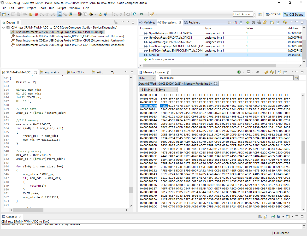
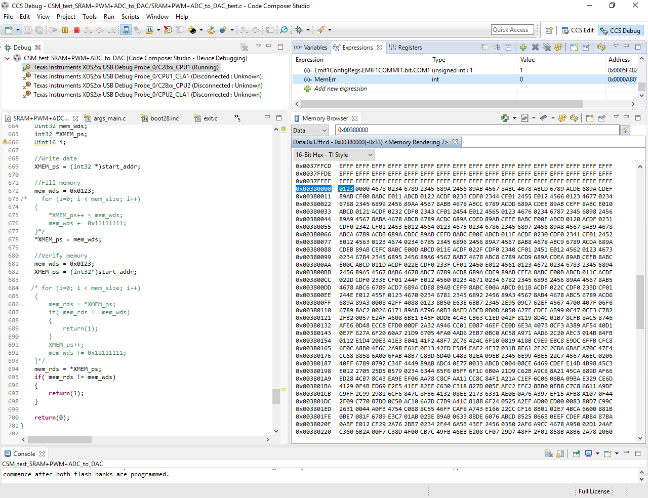
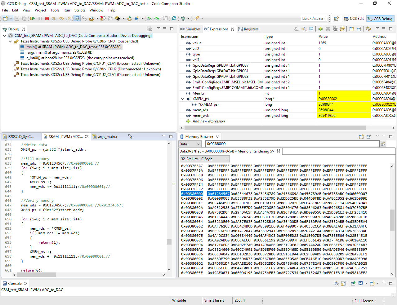
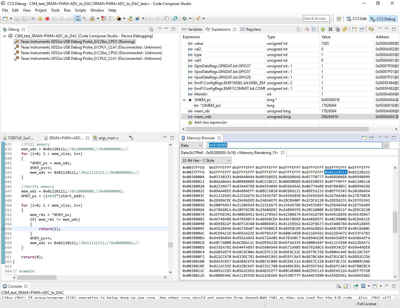
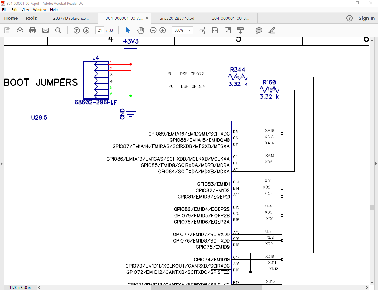
I am using 28377D and would like to talk with external SRAM ( ISSI IS61WV25616Axx/Bxx, 256k*16) for simple test. I read the example project (emif1_16bit_asram_cpu01) and understand about related register settings. But I did not see any explanation on address, which in this example starts from 0x100000 and has size of 0x8000. Since there is no specific information on external device, I wonder these numbers are made up or mean something. And how can I decide address and size of my own project, based on something? I have done settings of related registers, what else do I need to do, like cmd file?

Thanks!

Yi

  • Hi Zhang,

    Address 0x100000 is CS2 address space. Any access done to this address will be send to external devices connected via CS2. Each device is connected to specific chip select signal (in this case CS2) and that's how it get addressed.

    What is your usecase? Are you planning to store data during runtime in external device and access or some other usecase?

    Regards,

    Vivek Singh

  • Vivek,

    Thanks for the timely reply. I am using CS4 now and would like to do simple write and read test to external SRAM to make sure it is working, like what is done in example project. In the future, SRAM will be used as extra memory space for our project but right now I am just doing test plan for the board. So in my case, what address can I use and is there anything else to change for cmd file?

    Thanks,
    Yi
  • Hi,

    Another question is about read/write enable. Take read as example: here is what reference manual says "at start of set up period, EM1CS[4:2] falls to enable the external device". Since it is GPIO pin function as EM1CS4, how often do we change its value to enable external device, each time enable then disable when talking to device or just once? What about read enable and write enable, is it periodically and manually or just once? I am confused about this since it seems CPU did not talk well with SRAM in my project, and I do not know how to observe value in those addresses.

    Thanks.
  • Hi Zhang,

    Address for CS4 is 0x380000. It has been mentioned in section "6.3.3 EMIF Chip Select Memory Map" in device Datasheet. Example you are referring programs registers related to CS2 but you are using CS4 so you need to program EMIF registers related to CS4.

    Read/Write enables are also EMIF pins and are driven by EMIF IP (need to configure the mux to select them as EMIF). User need not to worry about toggling these pins.

    Regards,

    Vivek Singh

  • Vivek,

    I programmed CS4 related registers and configured related GPIO pins for EMIF  function. So we do not need to change value for chip enable and read/write enable pins, right? But now I used similar read/write program as example except for some small changes to CS4, it did not work well. Is there any way I can have access to values written in those addresses or debug what is wrong?

    Also I have question about this function. Since SRAM is set for 16bit, is it OK to write 32bit value, eg:0x01234567?

    Attached is the program for your reference.

    Thanks,

    Yi

  • Hi,

    Also I have question about this function. Since SRAM is set for 16bit, is it OK to write 32bit value, eg:0x01234567?

    Yes, that is ok.

    What is the value of start_addr in code ?

    Vivek Singh

  • Hi,

    I called the function like this : 

    MemErr = SRAM_Test(start,size);  

    Uint32 start = 0x00380000;  // start address of SRAM, CS4 space

    Uint32 size = 0x80;   // size of SRAM, 0x10000=64k

    But it seems that writing is not successful, since return value is always 1 which means write value is not equal to read value. But I did not figure out what is wrong.

  • Can you open memory browser window in CCS and try to write at 0x380000 address directly from there instead of code and see what happens?
  • Hi,

    I checked the memory browser and there is indeed value written at those addresses, but still returns error. I wonder what you means by directly writing at those addresses.

  • Sorry, the attached picture is wrong and this one is the real one I mentioned, which is similar to example and still does not work.

    Thanks.

  • Hi,

    In addition, I just tried to write single 32/16 bit value at the address and read to check it. This time return 0 which means no error. I wonder if there is something wrong with the write/read for loop. Can you give some hints? I really appreciate it.

  • Please set a breakpoint on return(1) code and check the value of XMEM_ps (address) and mem_rds and mem_wds. This will tell which address is failing and the difference in read and write data.
  • I can set the breakpoint but cannot add those expressions which show unknown. And should I just "run" or use "step over"? I am not very good at debugging, sorry for these silly questions.

  • These must be local variables hence you'll not be able to see them unless CPU halts inside the function. After setting the breakpoint, run the code.
  • Hi,

    I set the breakpoint and run, then it shows as following. "MemErr" changes to 1, indicating an error, but I cannot observe the variable values or data in those addresses. Is there a way to see what happens?

  • Hi,

    I changed those variables to global to observe values and the program fails at 0x00380002 when increasing 0x11111111 each time. But what is weird is that when increasing 0x1 each time, the program turns out to be fine.  It seems that increasing 0x11111111 results in overlimit or something, but it only happens at read value loop not write value loop, since it can write correctly for all addresses. Can you give any hints on what happens? I am really confused about it. The following two captures are two cases, first is good one and second is failed one.

    Thanks,

    Yi

  • I tried several different increasing numbers and it seems there is something wrong with the 8th and 4th bit. Since error always occurs when these bits need to increase 1, sometimes because of lower bits are full. I tried increasing 0x01110111 and the following capture shows what happend. I wonder whether the storage logic is not that straightforward and I need to pay more attention on some settings, or there is something wrong with the SRAM chip.... I am confused about this. Hope you can give some hints. Really appreciate it.

  • I think you mean 13th bit (D12). Right?

    Please check pinmux setting to make sure this pin is configured as EMIF pin. This should be ok but just double check.

    I am suspecting some issue on the board while connecting the SRAM. Do the connectivity check for this particular pin on board.

    Regards,

    Vivek Singh

  • Hi,

    Thanks a lot for the advice. It is D12 that I mentioned. I tried to avoid that data pin by increasing 0x20002000 each time and it is fine for now. At least this can prove SRAM is talking with DSP, right? I still need to check pin D12, which seems to be connected to another device too.
  • Hi Zhang,

     I tried to avoid that data pin by increasing 0x20002000 each time and it is fine for now. At least this can prove SRAM is talking with DSP, right?

    That is correct. Look like issue with D12 on board and fixing that should solve the issue.

    Regards,

    Vivek Singh

  • Hi Singh,

    I found the problem with D12, but have no idea how this affects the EMIF function. D12(GPIO72) is also used as pin for boot mode, and the connection is shown below. At this moment, I am afraid that we cannot change this connection. But I wonder how this conflict happens since we did nothing for GPIO72 setting except for the hardware connection in boot mode. Can you give some hints?

  • This was further discussed here and resolved.