


Hi Champs,
My customer had an application. Their product will be used in parallel.
They use GPIO pin to connected an signal bus directly as bellowing block diagram.
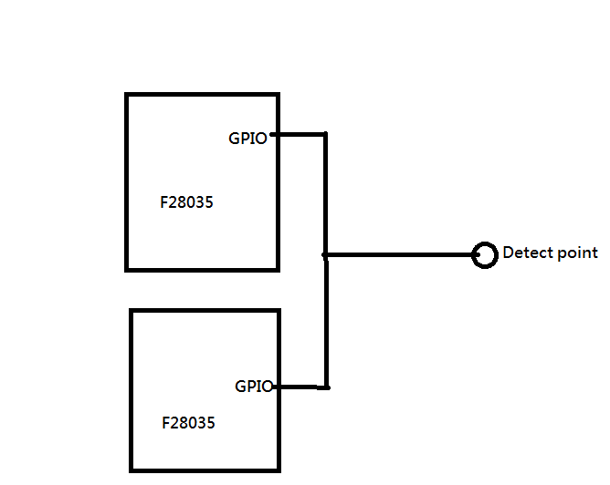
The GPIO pins were configured as output pin and the pull up module was disable.
They need to have one GPIO was set high initilally and the another will pull down the bus.
We use GPIO module to test firstly at single unit and we fund the voltage was not zero.
The dropping voltage will be kept at 1.49V as the bellowing waveform.
The original was 3.3V and the voltage will be dropping to 1.49V when we clear another GPIO DAT value.
At this condition , one is GPIO12 and another GPIO31
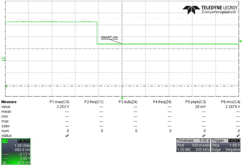
However , Only GPIO18 will pull down the voltage bellowing 1V.

Customer want to know why the GPIO can not really pull down the voltage to zero and why there was difference between pins.
But also what was the block diagram of the GPIO module at C2000 ?
Did you have any suggestion for the configuration?
BR
Brian
