Other Parts Discussed in Thread: C2000WARE
Tool/software: Code Composer Studio
Hello,
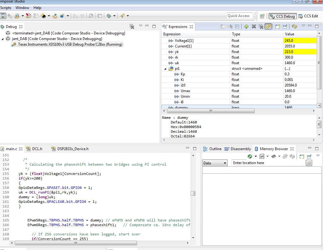
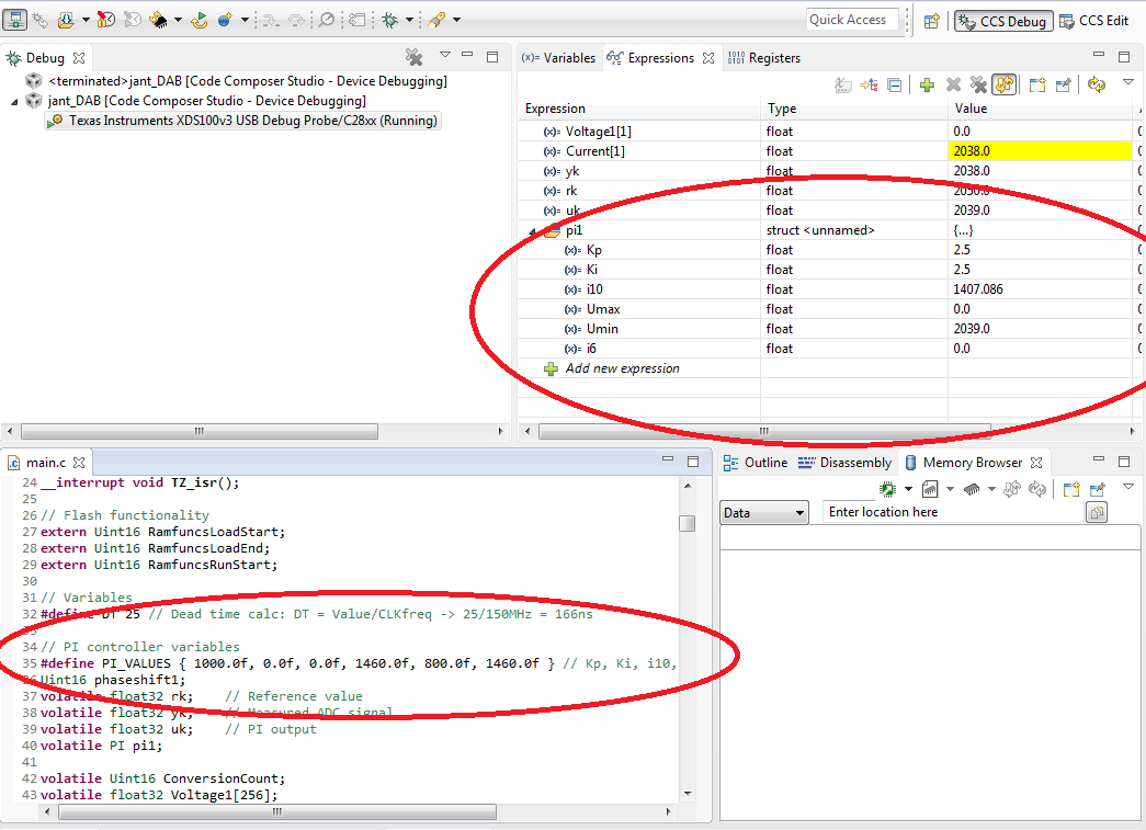
I am trying to implement your Digital Controller Library on the F28335 following the guidelines from SPRUI31. However, no matter my settings or values for KP, KI, upper/lower saturation, the values within my PI struct seem to be different. I believe I have a misconception on how to use and understand the library and would therefore appreciate your help. I am using phaseshift control between two bridges, where the phaseshift between two PWM channels is supposed to be between 800 and 1460 within the phaseshift register. Hence I set the saturation limits to 800 and 1460. I start with Kp=10 and disable the integrator to have a purely P regulator (the Ki parameters will be adjusted in a later stage to properly control the DCDC converter). These values are defined in PI_VALUES as shown in the C code given below.
The ADC interrupt service routine works properly and the ADC readings work properly as well. Debugging the code, I can see that the PI function is also called and the DCL_PI.asm code is executed. By inspecting the values of my PI regulator, I can see that the value differ from my settings. Also, I can see that the output of the PI regulator is clamped to Umin, which is the lower saturation bound to b e 2039 as opposed to be 800 in my settings. Do you have any idea of what is happening and what I am doing wrong? I would appreciate your guidance.
#include "DSP28x_Project.h"
#include "DCL.h"
void InitialADC();
void InitePWM1();
void InitePWM2();
void InitePWM5();
void InitePWM6();
__interrupt void ADC_isr();
__interrupt void TZ_isr();
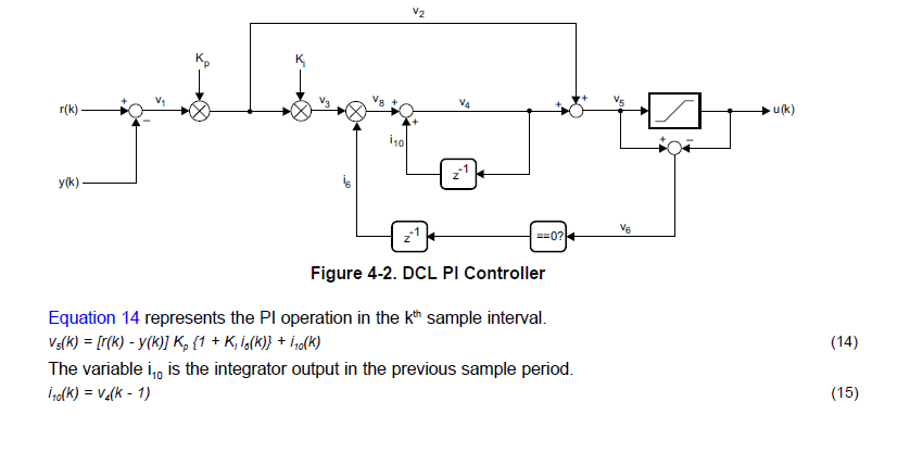
// Flash functionality
extern Uint16 RamfuncsLoadStart;
extern Uint16 RamfuncsLoadEnd;
extern Uint16 RamfuncsRunStart;
// Variables
#define DT 25 // Dead time calc: DT = Value/CLKfreq -> 25/150MHz = 166ns
Uint16 phaseshift1;
// PI controller variables
#define PI_VALUES { 1000.0f, 0.0f, 0.0f, 1460.0f, 800.0f, 1460.0f } // Kp, Ki, i10, Sat_max, Sat_min, Sat_storage
volatile float32 rk; // Reference value
volatile float32 yk; // Measured ADC signal
volatile float32 uk; // PI output
volatile PI pi1;
volatile Uint16 ConversionCount;
volatile float32 Voltage1[256];
volatile float32 Current[256];
void main(void) {
// Initialize PLL, Watchdog, enable peripheral clocks
InitSysCtrl();
// Used to program to flash
MemCopy(&RamfuncsLoadStart, &RamfuncsLoadEnd, &RamfuncsRunStart);
// Initialize ePWM and TZ
InitEPwmGpio();
InitTzGpio();
// Initialize PIE control registers
InitPieCtrl();
IER = 0x0000;
IFR = 0x0000;
// Initialize PIE vector table to default ISR
InitPieVectTable();
// Remap the ISR function to the PIE vector table
EALLOW;
PieVectTable.ADCINT = &ADC_isr;
PieVectTable.EPWM1_TZINT = &TZ_isr;
EDIS;
// First step of setting up the ADC sampling rate
EALLOW;
SysCtrlRegs.HISPCP.all = 3; // HSPCLK = SYSCLKOUT/2*ADC_MODCLK2 = 150/(2*3) = 25.0 MHz
EDIS;
// Synchronization already done in the InitSysCtrl() function --> Ask the TI support to verify
/*
EALLOW;
SysCtrlRegs.PCLKCR0.bit.TBCLKSYNC = 1; // Enable time base clock synchronization with SYSCLKOUT from DSP
EDIS;
*/
InitFlash();
ConversionCount = 0; // Initialize the count
uk = 0;
rk = 2050; // Approx. 5A load voltage
PI pi1 = PI_VALUES; // Initialize the PI controller
// Initialize the ADC
InitAdc();
phaseshift1 = 5; // Compensating a ca. 15ns delay between ePWM1 and ePWM6
InitialADC(); // Set up the ADC for voltage and current measurement
EALLOW;
SysCtrlRegs.PCLKCR0.bit.TBCLKSYNC = 0;
EDIS;
InitePWM1();
InitePWM2();
InitePWM5();
InitePWM6();
EALLOW;
SysCtrlRegs.PCLKCR0.bit.TBCLKSYNC = 1;
EDIS;
/*
* Set GPIO4 as output to measure execution time within ISR
*/
EALLOW;
// Set GPIO10 as a GPIO - already done in InitGpio()
GpioCtrlRegs.GPAMUX1.bit.GPIO4 = 0;
// Set GPIO10 as an output
GpioCtrlRegs.GPADIR.bit.GPIO4 = 1;
EDIS;
PieCtrlRegs.PIEIER1.bit.INTx6 = 1; // Group 1, bit 6 for ADC
PieCtrlRegs.PIEIER2.bit.INTx1 = 1; // Group 2, bit 1 for ePWM1_TZ
IER |= M_INT1; // Sets the interrupt enable bit of group 1
IER |= M_INT2; // Sets the interrupt enable bit of group 3
EINT; // Enable global interrupts INTM
for(;;)
{
}
}
__interrupt void ADC_isr(void)
{
GpioDataRegs.GPASET.bit.GPIO4 = 1;
Voltage1[ConversionCount] = AdcRegs.ADCRESULT0 >>4; // Read value from ADCINA5
Current[ConversionCount] = AdcRegs.ADCRESULT1 >>4; // Read value from ADCINB5
if(Current[ConversionCount]>2800)
{
// Overcurrent - Stop DAB converter
EPwm1Regs.CMPA.half.CMPA = 0;
EPwm2Regs.CMPA.half.CMPA = 1500;
EPwm6Regs.CMPA.half.CMPA = 0;
EPwm5Regs.CMPA.half.CMPA = 1500;
}
/*
* Calculating the phaseshift between two bridges using PI control
*/
yk = Current[ConversionCount];
uk = DCL_runPI(&pi1,rk,yk);
EPwm5Regs.TBPHS.half.TBPHS = uk; // ePWM5 and ePWM6 will have phaseshift
EPwm6Regs.TBPHS.half.TBPHS = phaseshift1; // Compensate ca. 16ns delay of ePWM6
// If 256 conversions have been logged, start over
if(ConversionCount == 255)
{
ConversionCount = 0;
}
else
{
ConversionCount++;
}
// Re-initialize for next ADC
AdcRegs.ADCTRL2.bit.RST_SEQ1 = 1; // Reset SEQ1
AdcRegs.ADCST.bit.INT_SEQ1_CLR = 1; // Clears the interrupt flag bit
PieCtrlRegs.PIEACK.all = PIEACK_GROUP1; // Acknowledge interrupt to PIE
GpioDataRegs.GPACLEAR.bit.GPIO4 = 1;
}
__interrupt void TZ_isr(void)
{
// Clear interrupt flag
EALLOW;
EPwm1Regs.TZCLR.bit.OST = 1;
EPwm2Regs.TZCLR.bit.OST = 1;
EPwm5Regs.TZCLR.bit.OST = 1;
EPwm6Regs.TZCLR.bit.OST = 1;
EPwm1Regs.TZCLR.bit.INT = 1;
EDIS;
PieCtrlRegs.PIEACK.all = PIEACK_GROUP2; // Acknowledge interrupt to PIE
}
void InitialADC(void)
{
// Configure ADC
AdcRegs.ADCTRL3.bit.ADCCLKPS = 1; // Set the ADC sampling rate: 25MHz/(2*1+1) = 8.3MHz
AdcRegs.ADCTRL1.bit.ACQ_PS = 0; //
AdcRegs.ADCTRL1.bit.SEQ_CASC = 0; // Cascaded mode
AdcRegs.ADCTRL1.bit.CONT_RUN = 0; // Start-stop mode
AdcRegs.ADCTRL3.bit.SMODE_SEL = 1; // Simultaneous sampling mode
AdcRegs.ADCTRL2.bit.EPWM_SOCA_SEQ1 = 1; // ePWM starts SOCA trigger
AdcRegs.ADCMAXCONV.bit.MAX_CONV1 = 0; // One conversion
AdcRegs.ADCCHSELSEQ1.bit.CONV00 = 5; // ADCINA5 and ADCINB5
AdcRegs.ADCTRL2.bit.INT_ENA_SEQ1 = 1; // Interrupt request enabled
}
void InitePWM1(void)
{
// Enable SOCA for ADC measurements
EPwm1Regs.ETSEL.bit.SOCAEN = 1; // Enable SOCA
EPwm1Regs.ETSEL.bit.SOCASEL = 4; // Generate SOCA pulse at 50% duty cycle
EPwm1Regs.ETPS.bit.SOCAPRD = 1; // Generate pulse on 1st event
EPwm1Regs.TBPRD = 1499; // Set the PWM period time
EPwm1Regs.CMPA.half.CMPA = (1499+1)/2;
EPwm1Regs.TBPHS.half.TBPHS = 0; // Set Phase register to zero
EPwm1Regs.TBCTL.bit.CTRMODE = TB_COUNT_UP; // Up count mode
EPwm1Regs.TBCTL.bit.PHSEN = TB_DISABLE; // Master module
EPwm1Regs.TBCTL.bit.PRDLD = TB_SHADOW;
EPwm1Regs.TBCTL.bit.SYNCOSEL = TB_CTR_ZERO; // Sync down-stream module
EPwm1Regs.TBCTL.bit.HSPCLKDIV = 0; // Set time base clock to SYSCLKOUT
EPwm1Regs.CMPCTL.bit.SHDWAMODE = CC_SHADOW;
EPwm1Regs.CMPCTL.bit.SHDWBMODE = CC_SHADOW;
EPwm1Regs.CMPCTL.bit.LOADAMODE = 0; // Loads on either CTR=0 or CTR=PRD
EPwm1Regs.CMPCTL.bit.LOADBMODE = 0; // Loads on either CTR=0 or CTR=PRD
EPwm1Regs.AQCTLA.bit.ZRO = AQ_SET; // Sets pin when CTR=PRD
EPwm1Regs.AQCTLA.bit.CAU = AQ_CLEAR; // Clears pin when CTR=COMPA
EALLOW;
EPwm1Regs.TZSEL.bit.OSHT3 = 1; // Enable TZ3
EPwm1Regs.TZCTL.bit.TZA = 2; // Clear ePWM1A on TZ event
EPwm1Regs.TZCTL.bit.TZB = 2; // Clear ePWM1B on TZ event
EPwm1Regs.TZEINT.bit.OST = 1; // Enable interrupt generation
EDIS;
EPwm1Regs.DBCTL.bit.IN_MODE = 0; // ePWMxA source for falling and rising edge
EPwm1Regs.DBCTL.bit.OUT_MODE = DB_FULL_ENABLE; // DB full enable
EPwm1Regs.DBCTL.bit.POLSEL = DB_ACTV_HIC; // Active high complementary
EPwm1Regs.DBRED = DT;
EPwm1Regs.DBFED = DT;
}
void InitePWM2(void)
{
EPwm2Regs.TBPRD = 1499; // Set the PWM period time
EPwm2Regs.CMPA.half.CMPA = (1499+1)/2;
EPwm2Regs.TBPHS.half.TBPHS = 0; // Set Phase register to zero
EPwm2Regs.TBCTL.bit.CTRMODE = TB_COUNT_UP; // Up count mode
EPwm2Regs.TBCTL.bit.PHSEN = TB_ENABLE; // Master module
EPwm2Regs.TBCTL.bit.PRDLD = TB_SHADOW;
EPwm2Regs.TBCTL.bit.SYNCOSEL = TB_CTR_ZERO; // Sync down-stream module
EPwm2Regs.TBCTL.bit.HSPCLKDIV = 0; // Set time base clock to SYSCLKOUT
EPwm2Regs.CMPCTL.bit.SHDWAMODE = CC_SHADOW;
EPwm2Regs.CMPCTL.bit.SHDWBMODE = CC_SHADOW;
EPwm2Regs.CMPCTL.bit.LOADAMODE = 0; // Loads on either CTR=0 or CTR=PRD
EPwm2Regs.CMPCTL.bit.LOADBMODE = 0; // Loads on either CTR=0 or CTR=PRD
EPwm2Regs.AQCTLA.bit.ZRO = AQ_CLEAR; // Clears pin when CTR=PRD
EPwm2Regs.AQCTLA.bit.CAU = AQ_SET; // Sets pin when CTR=COMPA
EALLOW;
EPwm2Regs.TZSEL.bit.OSHT3 = 1; // Enable TZ3
EPwm2Regs.TZCTL.bit.TZA = 2; // Clear ePWM2A on TZ event
EPwm2Regs.TZCTL.bit.TZB = 2; // Clear ePWM2B on TZ event
EDIS;
EPwm2Regs.DBCTL.bit.IN_MODE = 0; // ePWMxA source for falling and rising edge
EPwm2Regs.DBCTL.bit.OUT_MODE = DB_FULL_ENABLE; // DB full enable
EPwm2Regs.DBCTL.bit.POLSEL = DB_ACTV_HIC; // Active high complementary
EPwm2Regs.DBRED = DT;
EPwm2Regs.DBFED = DT;
}
void InitePWM5(void)
{
EPwm5Regs.TBPRD = 1499; // Set the PWM period time
EPwm5Regs.CMPA.half.CMPA = (1499+1)/2;
EPwm5Regs.TBPHS.half.TBPHS = 0; // Set Phase register to zero
EPwm5Regs.TBCTL.bit.CTRMODE = TB_COUNT_UP; // Up count mode
EPwm5Regs.TBCTL.bit.PHSEN = TB_ENABLE; // Slave module
EPwm5Regs.TBCTL.bit.PRDLD = TB_SHADOW;
EPwm5Regs.TBCTL.bit.SYNCOSEL = TB_CTR_ZERO; // Sync down-stream module
EPwm5Regs.TBCTL.bit.HSPCLKDIV = 0; // Set time base clock to SYSCLKOUT
EPwm5Regs.CMPCTL.bit.SHDWAMODE = CC_SHADOW;
EPwm5Regs.CMPCTL.bit.SHDWBMODE = CC_SHADOW;
EPwm5Regs.CMPCTL.bit.LOADAMODE = 0; // Loads on either CTR=0 or CTR=PRD
EPwm5Regs.CMPCTL.bit.LOADBMODE = 0; // Loads on either CTR=0 or CTR=PRD
EPwm5Regs.AQCTLA.bit.ZRO = AQ_CLEAR; // Clears pin when CTR=PRD
EPwm5Regs.AQCTLA.bit.CAU = AQ_SET; // Sets pin when CTR=COMPA
EALLOW;
EPwm5Regs.TZSEL.bit.OSHT3 = 1; // Enable TZ3
EPwm5Regs.TZCTL.bit.TZA = 2; // Clear ePWM5A on TZ event
EPwm5Regs.TZCTL.bit.TZB = 2; // Clear ePWM5B on TZ event
EDIS;
EPwm5Regs.DBCTL.bit.IN_MODE = 0; // ePWMxA source for falling and rising edge
EPwm5Regs.DBCTL.bit.OUT_MODE = DB_FULL_ENABLE; // DB full enable
EPwm5Regs.DBCTL.bit.POLSEL = DB_ACTV_HIC; // Active high complementary
EPwm5Regs.DBRED = DT;
EPwm5Regs.DBFED = DT;
}
void InitePWM6(void)
{
EPwm6Regs.TBPRD = 1499; // Set the PWM period time
EPwm6Regs.CMPA.half.CMPA = (1499+1)/2;
EPwm6Regs.TBPHS.half.TBPHS = 0; // Set Phase register to zero
EPwm6Regs.TBCTL.bit.CTRMODE = TB_COUNT_UP; // Up count mode
EPwm6Regs.TBCTL.bit.PHSEN = TB_ENABLE; // Slave module
EPwm6Regs.TBCTL.bit.PRDLD = TB_SHADOW;
EPwm6Regs.TBCTL.bit.SYNCOSEL = TB_CTR_ZERO; // Sync down-stream module
EPwm6Regs.TBCTL.bit.HSPCLKDIV = 0; // Set time base clock to SYSCLKOUT
EPwm6Regs.CMPCTL.bit.SHDWAMODE = CC_SHADOW;
EPwm6Regs.CMPCTL.bit.SHDWBMODE = CC_SHADOW;
EPwm6Regs.CMPCTL.bit.LOADAMODE = 0; // Loads on either CTR=0 or CTR=PRD
EPwm6Regs.CMPCTL.bit.LOADBMODE = 0; // Loads on either CTR=0 or CTR=PRD
EPwm6Regs.AQCTLA.bit.ZRO = AQ_SET; // Sets pin when CTR=PRD
EPwm6Regs.AQCTLA.bit.CAU = AQ_CLEAR; // Clears pin when CTR=COMPA
EALLOW;
EPwm6Regs.TZSEL.bit.OSHT3 = 1; // Enable TZ3
EPwm6Regs.TZCTL.bit.TZA = 2; // Clear ePWM6A on TZ event
EPwm6Regs.TZCTL.bit.TZB = 2; // Clear ePWM6B on TZ event
EDIS;
EPwm6Regs.DBCTL.bit.IN_MODE = 0; // ePWMxA source for falling and rising edge
EPwm6Regs.DBCTL.bit.OUT_MODE = DB_FULL_ENABLE; // DB full enable
EPwm6Regs.DBCTL.bit.POLSEL = DB_ACTV_HIC; // Active low complementary
EPwm6Regs.DBRED = DT;
EPwm6Regs.DBFED = DT;
}