This thread has been locked.

If you have a related question, please click the "Ask a related question" button in the top right corner. The newly created question will be automatically linked to this question.

TMS320F28035: Blanking window doesn't blank from the beginning of the period with DCOFFSET = 0

Part Number: TMS320F28035

Hello

I'm trying to setup a blanking window on TMS320F28035. I have a CBC trip zone configured from COMP3 to trip PWM2. I want the blanking window to start right at the beginning of the pwm period and last over the dead time and until some time after the pulse starts. But if I set DCOFFSET to 0 it seems that a trip at the very end of a period can trip the next pulse before the blanking window is activated causing the whole pulse to disappear.

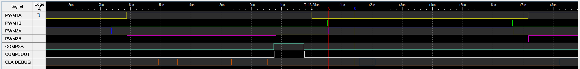
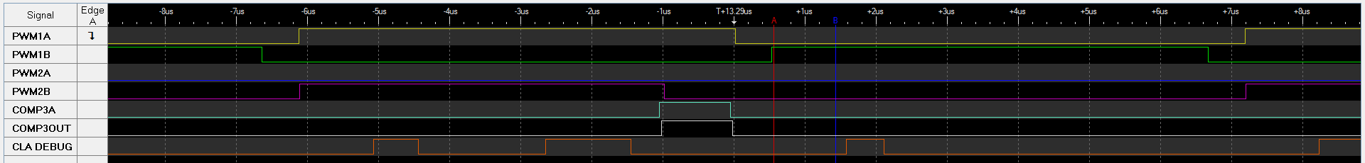
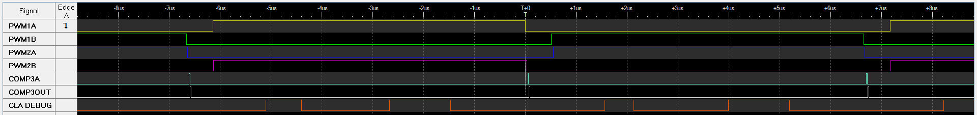
For testing I use a spare pwm connected to COMP3A and generate a sweeping pulse to see how the trip zone acts at different timings. On the first image the PWM2A and B pulses are still tripped normally but when I advance the test pulse right one step (second image) the PWMs are tripped before they have begun.

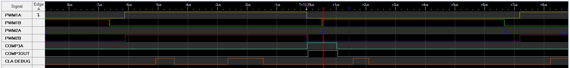
After advancing a few steps more (third image) the blanking window starts to work correctly and PWM2 pulses are started even if there is a trip during the dead time.

As a workaround, I can set the offset to TBPRD - 5 so that the blanking window actually starts from the end of the previous cycle, but I'm confused why it doesn't work with offset 0 as expected? The CBC trip should be cleared at the end of the period and it should not be possible to trip the next pulse? Or are there some other delays on the trip signal that I don't know of?

Best regards
Pauli

  • Hi Pauli,

    Do you mind posting your PWM configuration code? I would like to see how your trip and blanking window are configured, but please post the rest of the PWM setup as well.

    Thanks,

    Kris

  • I think here should be the relevant configurations for COMP3, PWM1 and PWM2. PWM2 is running at a double frequency compared to PWM1. Additionally there is a CLA task triggering itself again on both up and down slopes of PWM1 and making the alternate pulses on PWM2 to disappear. So we get identical pulse pattern as on PWM1, but so that PWM2 period ends and CBC trip zone resets after every single pulse.

    For the blanking window this is the setup that uses DCFOFFSET = 0 and doesn't blank from the beginning of the period as expected. The workaround used is in the commented out lines.

    EALLOW;
    SysCtrlRegs.PCLKCR3.bit.COMP3ENCLK = 1;

    Comp3Regs.COMPCTL.bit.SYNCSEL = 0;
    Comp3Regs.COMPCTL.bit.CMPINV = 0;
    Comp3Regs.COMPCTL.bit.COMPSOURCE = 0;
    Comp3Regs.COMPCTL.bit.COMPDACEN = 1;
    Comp3Regs.DACVAL.bit.DACVAL = 200;
    EDIS;


    EALLOW;
    // Time Base SubModule Registers
    EPwm1Regs.TBCTL.bit.PRDLD = TB_SHADOW;
    EPwm1Regs.TBPRD = (60000000 / (75000)) / 2;
    EPwm1Regs.TBPHS.half.TBPHS = 0;
    EPwm1Regs.TBCTR = 0;

    EPwm1Regs.TBCTL.bit.CTRMODE = TB_COUNT_UPDOWN;
    EPwm1Regs.TBCTL.bit.HSPCLKDIV = TB_DIV1;
    EPwm1Regs.TBCTL.bit.CLKDIV = TB_DIV1;

    // Counter Compare Submodule Registers
    EPwm1Regs.CMPA.half.CMPA = 74;
    EPwm1Regs.CMPB = 0;
    EPwm1Regs.CMPCTL.bit.SHDWAMODE = CC_IMMEDIATE;

    // Create fixed 50% PWM with Action Qualifiers
    EPwm1Regs.AQCTLA.bit.ZRO = AQ_SET;
    EPwm1Regs.AQCTLA.bit.PRD = AQ_CLEAR;

    EPwm1Regs.AQCTLB.bit.ZRO = AQ_SET;
    EPwm1Regs.AQCTLB.bit.PRD = AQ_CLEAR;

    // Active high complementary PWMs - Set up the deadband
    EPwm1Regs.DBCTL.bit.IN_MODE = DBA_ALL;
    EPwm1Regs.DBCTL.bit.OUT_MODE = DB_FULL_ENABLE;
    EPwm1Regs.DBCTL.bit.POLSEL = DB_ACTV_HIC;
    EPwm1Regs.DBRED = 31;
    EPwm1Regs.DBFED = 31;

    // Setup interrupt at CMPA to start CLA task1 (reconfigure PWM registers for next half cycle)
    EPwm1Regs.ETSEL.bit.INTSEL = ET_CTRU_CMPA;
    EPwm1Regs.ETSEL.bit.INTEN = 1;
    EPwm1Regs.ETPS.bit.INTPRD = ET_1ST;

    // Force both PWM pins low on trip (OST used for turning off PWM)
    EPwm1Regs.TZCTL.bit.TZA = TZ_FORCE_LO;
    EPwm1Regs.TZCTL.bit.TZB = TZ_FORCE_LO;

    // Enable sync output.
    EPwm1Regs.TBCTL.bit.SYNCOSEL = TB_CTR_ZERO;
    EDIS;


    EALLOW;
    // Time Base SubModule Registers
    EPwm2Regs.TBCTL.bit.PRDLD = TB_SHADOW;
    EPwm2Regs.TBPRD = (60000000 / (75000 * 2)) - 1;
    EPwm2Regs.TBPHS.half.TBPHS = 0;
    EPwm2Regs.TBCTR = 0;

    EPwm2Regs.TBCTL.bit.CTRMODE = TB_COUNT_UP;
    EPwm2Regs.TBCTL.bit.HSPCLKDIV = TB_DIV1;
    EPwm2Regs.TBCTL.bit.CLKDIV = TB_DIV1;

    EPwm2Regs.TBCTL.bit.PHSEN = TB_ENABLE;
    EPwm2Regs.TBCTL.bit.SYNCOSEL = TB_SYNC_IN;

    // Counter Compare Submodule Registers
    EPwm2Regs.CMPA.half.CMPA = 0;
    EPwm2Regs.CMPB = 0;
    EPwm2Regs.CMPCTL.bit.SHDWAMODE = CC_SHADOW;
    EPwm2Regs.CMPCTL.bit.LOADAMODE = CC_CTR_PRD;

    // AQCTLA and B are configured in CLA task 1
    EPwm2Regs.AQCTLA.bit.PRD = AQ_CLEAR;

    EPwm2Regs.AQCTLB.bit.PRD = AQ_CLEAR;

    // Force both PWM pins low on trip (OST used for turning off PWM. CBC trip trough DCAEVT2)
    EPwm2Regs.TZCTL.bit.TZA = TZ_FORCE_LO;
    EPwm2Regs.TZCTL.bit.TZB = TZ_FORCE_LO;
    EPwm2Regs.TZCTL.bit.DCAEVT1 = TZ_NO_CHANGE;
    EPwm2Regs.TZCTL.bit.DCAEVT2 = TZ_NO_CHANGE;
    EPwm2Regs.TZCTL.bit.DCBEVT1 = TZ_NO_CHANGE;
    EPwm2Regs.TZCTL.bit.DCBEVT2 = TZ_NO_CHANGE;

    // Active high complementary PWMs - Set up the deadband
    EPwm2Regs.DBCTL.bit.IN_MODE = DBA_ALL;
    EPwm2Regs.DBCTL.bit.OUT_MODE = DB_FULL_ENABLE;
    EPwm2Regs.DBCTL.bit.POLSEL = DB_ACTV_HIC;
    EPwm2Regs.DBRED = 31;
    EPwm2Regs.DBFED = 31;
    EDIS;


    EALLOW;
    // Define an event (DCAEVT2) based on Comparator 1 Output
    EPwm2Regs.DCTRIPSEL.bit.DCAHCOMPSEL = DC_COMP3OUT; // DCAH = Comparator output
    EPwm2Regs.TZDCSEL.bit.DCAEVT2 = TZ_DCAH_HI; // DCAEVT2 = DCAH high(will become active as Comparator output goes high)
    EPwm2Regs.TZSEL.bit.DCAEVT2 = TZ_ENABLE; // Enable DCAEVT2 to trip trough CBC

    // Configure blanking window
    EPwm2Regs.DCFCTL.bit.BLANKE = DC_BLANK_ENABLE;
    EPwm2Regs.DCFCTL.bit.SRCSEL = DC_SRC_DCAEVT2;
    EPwm2Regs.DCFCTL.bit.PULSESEL = DC_PULSESEL_ZERO;
    EPwm2Regs.DCFCTL.bit.BLANKINV = DC_BLANK_NOTINV;
    // Set offset so that it ends 5 cycles before the period ends.
    // EPwm2Regs.DCFOFFSET = EPwm2Regs.TBPRD - 5;
    EPwm2Regs.DCFOFFSET = 0;
    // Actual blanking window size is:
    // Advance from previous period + deadband + actual blanking from the start of the pulse
    // EPwm2Regs.DCFWINDOW = 5 + 31 + 49;
    EPwm2Regs.DCFWINDOW = 31 + 49;
    EPwm2Regs.DCACTL.bit.EVT2SRCSEL = DC_EVT_FLT; // Use filtered (blanking) version of event

    // Capture TBCTR value on trip event
    EPwm2Regs.DCCAPCTL.bit.CAPE = 1;
    EDIS;


    EALLOW;
    SysCtrlRegs.PCLKCR0.bit.TBCLKSYNC = 1; // Enable TBCLK synchronization
    EDIS;


    Best regards

    Pauli

  • Pauli,

    It's going to be a few days at least before I can try anything on this device, but I have a few questions and thoughts-

    - Can you mark a waveform with exactly where TBCTR = 0 occurs? There's a lot going on with the deadband settings and the PWMs in different counting operations, so I want it to be very clear where the trip occurs in relation to that.Maybe for debug we could even just toggle a PWM on TBCTR = 0 without all of the extra enhancements.
    - Can you run a test where COMP3A (or any CBC trip signal) is definitely active well before the PWM period completes and carries over into the start of the blanking window at TBCTR = 0? I'm suspecting that if a DCEVT trip is still active from the previous period that for safety the trip is taking priority since the trip didn't actually occur during the blanking window. I'll need to research the implementation a bit on this, but it's my first thought.

    - How are you viewing the COMP3A and COMP3OUT signals? How are those being routed to the PWM?

    Thanks for all of the information. Great debug so far.

    Kris

  • Ok, Here's a configuration where the B pulses are replaced by short pulses at the start of the period (ZRO = SET, CBU = CLEAR, (CMPB = 10))

    Here I've sliced one of the old images and added rough illustrations for the TBCTR slopes for the PWMs.

    PWM1A pulse starts at ZRO delayed by deadband and ends at PRD. PWM2A pulse starts at CAU (CMPA = 0) delayed by deadband and cla task1 (short bump shown in CLA DEBUG) alternates between CAU to SET PWM2A and to do nothing. B channels are active high complements of A.

    I'm using PWM5A to generate the sweeping test pulse and this is wired to COMP3A pin. GPIO34 is configured as COMP3OUT and both are connected to the logic analyzer.

    If I make the COMP3A pulse wider as you suggested it only makes the area where the undesired effect (next pulse disappears) wider.

    Here everything is fine. PWM2B has been tripped where COMP3A starts and PWM2A begins normally:

    Here COMP3A pulse end is near the end of the PWM2 period and PWM2A disappears. The blanking window offset is 0 so the period should be blanked right from the beginning of PWM2 period??

    Until the COMP3A pulse is no longer in the range of the previous period then PWM2A is as it should be again (blanked from the beginning):

    And here we are again in the state where COMP3A pulse is active after the blankin period and PWM2A gets tripped as it should:

    The unwanted real life scenario where this happens is when the ending of a pulse (tripped or not) generates some noise the peak current measurement input and then makes the next pulse disappear.

    Best regards

    Pauli

  • Pauli,

    I'm going to attempt to replicate what you are seeing on the same device. It will be next week before I'm able to start experiments. I'll be in touch if I need any further information.

    Regards,
    Kris