Other Parts Discussed in Thread: CONTROLSUITE
Are there any constraint that limits the implementation of DPWM0, DPWM1, DPWM2 (aka GDPWM, aka UDPWM) on the TMS320F2812 processor? If so, what processor can implement these modulation schemes? Was this issue fixed with the ePWM peripheral in subsequent C2000 chips?
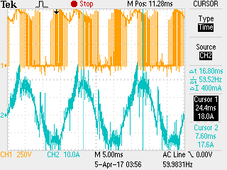
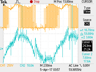
I am struggling to implement these schemes because of the PWM driver and/or PWM peripheral. It seems that I can't have 0% duty cycle (clamping to the negative bus). When I limit a compare register CMPR1..3 to timer 1 period T1PR, I am able to clamp to the negative bus, but the current waveform is distorted. If I limit a compare register CMPR1..3 to timer 1 period (T1PR - 1), the current waveform is satisfactory, but when the output is supposed to be clamped to the negative bus, there are pulses the width of the deadband time at intervals consistent with the switching frequency.
I found this thesis that claims that the TMS320F2812 isn't capable of some PWM methods. See pages 226/286. Is the following statement accurate?
"Loading the compare register with the duty cycle of the specific phase leg involves one instruction cycle of the DSP. In the TMS320F2812 the maximum clock cycle is 150 MHz which corresponds to 6.67 ns instruction cycle. This 6.67 ns delay causes problems in realizing various PWM methods. The problem arises when the calculated duty cycle is loaded to the counter at the period instant and its previous value is not 100% but the calculated value is 100%. This condition is encountered during implementation of discontinuous PWM methods and specifically either when loading with single update rate and at the period point or when loading with double update rate and at the period point. Since during loading at the period instant a delay 199 of 6.67ns exists, the opportunity for loading the correct duty cycle to the compare register is missed and a faulty signal which distorts the PWM waveforms and disturbs the output voltages/currents is generated."
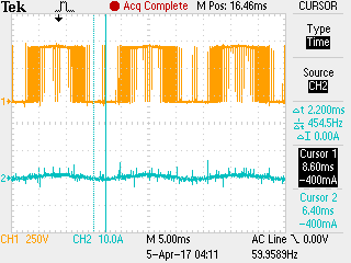
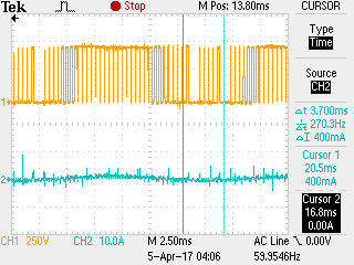
The following tests were performed with a 3-phase voltage source inverter, a fundamental frequency of 60 Hz, a switching frequency of 2.5 kHz and a rated motor voltage of 380V (l-l rms). Volts-per-Hertz mode is implemented. The PWM scheme is DPWM2.
When I implement the following PWM driver, I get the following current waveform which is satisfactory, but the pulses during the negative bus clamping period (60 degrees) yield a PWM scheme that doesn't fully realize the benefits of the reduction of switching losses of DPWM0, DPWM1, and/or DPWM2.
(NOTE 1: Since PWM1 is top IGBT, PWM2 is bottom IGBT and constraints on the PWM peripheral requires PWM1 to be active low and PWM2 to be active high in order to yield proper dead times, that means that the output of SVGEN modules will yield the opposite results (1 = 0% and -1 = 100%). Therefore, this inversion is accounted for in my pwm driver with ONE_Q24 - _IQdiv2(p->MfuncCx + ONE_Q24).
(NOTE 2: MfuncC1 is in Q24 format and ranges from -1 to 1 where -1 is 0% and 1 is 100%)
#define ONE_Q24 16777216 // _IQ24(1)
void F281X_EV1_DutyCycleUpdate(F281X_PWMGEN_ST *p)
{
		int32 Tmp1, Tmp2, Tmp3;

		// Set the timer period from the period modulation input
		EvaRegs.T1PR = p->PeriodMax;

		// Compute the compare 1 (Q0) from the PWM 1&2 duty cycle ratio (Q24)
		Tmp1 = ONE_Q24 - _IQdiv2(p->MfuncC1 + ONE_Q24);											// Convert from -1 to 1 to 0 to 1 scale
		Tmp1 = _IQsat(_IQ24mpy(Tmp1, (int32)EvaRegs.T1PR),(int32)(EvaRegs.T1PR - 1),0);

		// Compute the compare 2 (Q0) from the PWM 3&4 duty cycle ratio (Q24)
		Tmp2 = ONE_Q24 - _IQdiv2(p->MfuncC2 + ONE_Q24);											// Convert from -1 to 1 to 0 to 1 scale
		Tmp2 = _IQsat(_IQ24mpy(Tmp2, (int32)EvaRegs.T1PR),(int32)(EvaRegs.T1PR - 1),0);

		// Compute the compare 3 (Q0) from the PWM 5&6 duty cycle ratio (Q24)
		Tmp3 = ONE_Q24 - _IQdiv2(p->MfuncC3 + ONE_Q24);											// Convert from -1 to 1 to 0 to 1 scale
		Tmp3 = _IQsat(_IQ24mpy(Tmp3, (int32)EvaRegs.T1PR),(int32)(EvaRegs.T1PR - 1),0);

		EvaRegs.CMPR1 = (int16)Tmp1;
		EvaRegs.CMPR2 = (int16)Tmp2;
		EvaRegs.CMPR3 = (int16)Tmp3;

}


When I implement the following code (EvaRegs.T1PR - 1 goes to EvaRegs.T1PR), clamping to the negative bus is achieved, but the current waveform is distorted:
void F281X_EV1_DutyCycleUpdate(F281X_PWMGEN_ST *p)
{
		int32 Tmp1, Tmp2, Tmp3;

		// Set the timer period from the period modulation input
		EvaRegs.T1PR = p->PeriodMax;

		// Compute the compare 1 (Q0) from the PWM 1&2 duty cycle ratio (Q24)
		Tmp1 = ONE_Q24 - _IQdiv2(p->MfuncC1 + ONE_Q24);											// Convert from -1 to 1 to 0 to 1 scale
		Tmp1 = _IQsat(_IQ24mpy(Tmp1, (int32)EvaRegs.T1PR),(int32)(EvaRegs.T1PR),0);

		// Compute the compare 2 (Q0) from the PWM 3&4 duty cycle ratio (Q24)
		Tmp2 = ONE_Q24 - _IQdiv2(p->MfuncC2 + ONE_Q24);											// Convert from -1 to 1 to 0 to 1 scale
		Tmp2 = _IQsat(_IQ24mpy(Tmp2, (int32)EvaRegs.T1PR),(int32)(EvaRegs.T1PR),0);

		// Compute the compare 3 (Q0) from the PWM 5&6 duty cycle ratio (Q24)
		Tmp3 = ONE_Q24 - _IQdiv2(p->MfuncC3 + ONE_Q24);											// Convert from -1 to 1 to 0 to 1 scale
		Tmp3 = _IQsat(_IQ24mpy(Tmp3, (int32)EvaRegs.T1PR),(int32)(EvaRegs.T1PR),0);

		EvaRegs.CMPR1 = (int16)Tmp1;
		EvaRegs.CMPR2 = (int16)Tmp2;
		EvaRegs.CMPR3 = (int16)Tmp3;

}
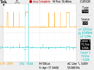
This second version of the pwm driver comes with another issue. If the modulation scheme is changed from UDPWM (set to DPWM2) to SVPWM (aka continuous PWM) and the bus voltage applied is insufficient to supply the rated motor voltage of 380V (VDC <= 537V), the modulation factor (SQRT(Vd^2 + Vq^2 or svgenMF.Gain from SVGENMF module) goes to 100% and there are spurious 200us pulses that are present when the duty cycle should be 0%. This is shown in the following scope captures. Note that 200 us is 1/2 the switching period (400 us = 2.5 kHz)
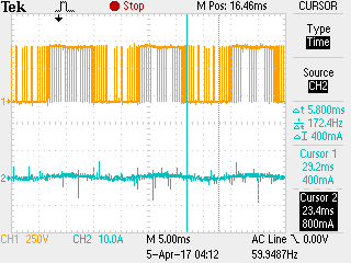
Reverting back to the first pwm driver does not demonstrate this phenomena: