Part Number: TMS320F28377S
Tool/software: Code Composer Studio
Hello.
I'm trying to understand the operation of the AD converter Post-processing blocks.
With a project from the C2000 Multi-Day Workshop, that one that uses the AD converter (Lab6), I'm try to put the PPB block to work.
If I associate the PPB1 with the SOC0, it doesn't work, but if I associate it with SOC1, works fine.
The SOC0 conversion is triggered by EPWM2. After the conversion, an interrupt is called to put the conversion results in the AdcBuf and AdcBuf2 variables.
AdcBuf save AdcaResultRegs.ADCRESULT0 and AdcBuf2 save AdcaResultRegs.ADCRESULT1.
To test the PPB block, I made two conversions, one started by the SOC0 and other by SOC1 and I associated first the PPB1 to SOC0.
The part of the code with this config is below.
//--- SOC0 and SOC1 configuration
	AdcaRegs.ADCSOC0CTL.bit.TRIGSEL = 7;		// SOC0 is triggered by the ePWM2 SOCA
	AdcaRegs.ADCSOC0CTL.bit.CHSEL = 0;			// SOC0 converts input ADCINA0 in single-sample mode
	AdcaRegs.ADCSOC0CTL.bit.ACQPS = 19;			// Acquisition window has a 20 SYSCLK cycle
    AdcaRegs.ADCSOC1CTL.bit.TRIGSEL = 7;        // SOC0 is triggered by the ePWM2 SOCA
    AdcaRegs.ADCSOC1CTL.bit.CHSEL = 0;          // SOC0 converts input ADCINA0 in single-sample mode
    AdcaRegs.ADCSOC1CTL.bit.ACQPS = 19;         // Acquisition window has a 20 SYSCLK cycle

//--- ADCA1 interrupt configuration
	AdcaRegs.ADCINTSEL1N2.bit.INT1CONT = 1;		// Interrupt pulses
	AdcaRegs.ADCINTSEL1N2.bit.INT1E = 1;		// ADC interrupt enable
	AdcaRegs.ADCINTSEL1N2.bit.INT1SEL = 1;		// EOC1 triggers the interrupt

//--- Enable the ADC interrupt
	PieCtrlRegs.PIEIER1.bit.INTx1 = 1;          // Enable ADCA1 interrupt in PIE group 1
	IER |= 0x0001;                              // Enable INT1 in IER to enable PIE group

//--- Setup PPB Offset
	AdcaRegs.ADCPPB1CONFIG.bit.CONFIG = 0;      //PPB1 is associated with SOC0
    AdcaRegs.ADCPPB1OFFCAL.all = 400;           //PPB1 will subtract OFFCAL value
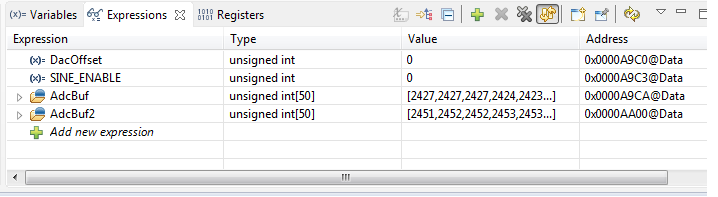
As you can see in the image, AdcBuf and AdcBuf2 are almost equal, indicating that PPB1 is not modifying AdcaResultRegs.ADCRESULT0
When PPB1 is associated to SOC1 by change AdcaRegs.ADCPPB1CONFIG.bit.CONFIG = 1, the values are modified as you can see in the next image.

So, my question is: Why PPB1, when asscoiated with SOC0, don't alter the AdcaResultRegs.ADCRESULT0 value?
I'm using Code Composer Studio V7.1.0 with C2000 Ware and LAUNCHXL-F28377S.
The complete code for AD config and adca interrupt is next.
void InitAdca(void)
{
	asm(" EALLOW");						// Enable EALLOW protected register access

//--- Reset the ADC.  This is good programming practice.
	DevCfgRegs.SOFTPRES13.bit.ADC_A = 1;	// ADC is reset
	DevCfgRegs.SOFTPRES13.bit.ADC_A = 0;	// ADC is released from reset

//--- Configure the ADC base registers
	AdcaRegs.ADCCTL1.all = 0x0004;		// Main ADC configuration
	AdcaRegs.ADCCTL2.all = 0x0006;		// ADC clock configuration
	AdcaRegs.ADCBURSTCTL.all = 0x0000;

//--- Call AdcSetMode() to configure the resolution and signal mode.
//    This also performs the correct ADC calibration for the configured mode.
    AdcSetMode(ADC_ADCA, ADC_RESOLUTION_12BIT, ADC_SIGNALMODE_SINGLE);

//--- SOC0 configuration
	AdcaRegs.ADCSOC0CTL.bit.TRIGSEL = 7;		// SOC0 is triggered by the ePWM2 SOCA
	AdcaRegs.ADCSOC0CTL.bit.CHSEL = 0;			// SOC0 converts input ADCINA0 in single-sample mode
	AdcaRegs.ADCSOC0CTL.bit.ACQPS = 19;			// Acquisition window has a 20 SYSCLK cycle
    AdcaRegs.ADCSOC1CTL.bit.TRIGSEL = 7;        // SOC0 is triggered by the ePWM2 SOCA
    AdcaRegs.ADCSOC1CTL.bit.CHSEL = 0;          // SOC0 converts input ADCINA0 in single-sample mode
    AdcaRegs.ADCSOC1CTL.bit.ACQPS = 19;         // Acquisition window has a 20 SYSCLK cycle

//--- ADCA1 interrupt configuration
	AdcaRegs.ADCINTSEL1N2.bit.INT1CONT = 1;		// Interrupt pulses
	AdcaRegs.ADCINTSEL1N2.bit.INT1E = 1;		// ADC interrupt enable
	AdcaRegs.ADCINTSEL1N2.bit.INT1SEL = 0;		// EOC0 triggers the interrupt

//--- Enable the ADC interrupt
	PieCtrlRegs.PIEIER1.bit.INTx1 = 1;          // Enable ADCA1 interrupt in PIE group 1
	IER |= 0x0001;                              // Enable INT1 in IER to enable PIE group

//--- Setup PPB Offset
	AdcaRegs.ADCPPB1CONFIG.bit.CONFIG = 0;      //PPB1 is associated with SOC0
    AdcaRegs.ADCPPB1OFFCAL.all = 400;           //PPB1 will subtract OFFCAL value

//--- Finish up
	AdcaRegs.ADCCTL1.bit.ADCPWDNZ = 1;			// Power up the ADC
	DELAY_US(1000);								// Wait 1 ms after power-up before using the ADC
	asm(" EDIS");								// Disable EALLOW protected register access

} // end InitAdc()
The adca interrupt is next.
interrupt void adca1_isr(void)                      // PIE1.1 @ 0x000D40  ADC-A interrupt #1
{
static Uint16 *AdcBufPtr = AdcBuf;                  // Pointer to buffer
static Uint16 *AdcBufPtr2 = AdcBuf2;                // Pointer to buffer 2
static Uint16 iQuadratureTable = 0;                 // Quadrature table index
static volatile Uint16 GPIO34_count = 0;            // Counter for pin toggle

    PieCtrlRegs.PIEACK.all = PIEACK_GROUP1;         // Must acknowledge the PIE group

//--- Manage the ADC registers
    AdcaRegs.ADCINTFLGCLR.bit.ADCINT1 = 1;          // Clear ADCINT1 flag

//--- Read the ADC result
    *AdcBufPtr++ =  AdcaResultRegs.ADCRESULT0;          // Read the result
    *AdcBufPtr2++ =  AdcaResultRegs.ADCRESULT1;          // Read the result

//--- Brute-force the circular buffer
    if( AdcBufPtr == (AdcBuf + ADC_BUF_LEN) )
    {
        AdcBufPtr = AdcBuf;                     // Rewind the pointer to beginning
        AdcBufPtr2 = AdcBuf2;
    }

//--- Example: Toggle GPIO18 so we can read it with the ADC ***/
    if(DEBUG_TOGGLE == 1)
    {
        GpioDataRegs.GPATOGGLE.bit.GPIO18 = 1;      // Toggle the pin
    }

//--- Example: Toggle GPIO34 at a 0.5 sec rate (connected to the LED on the ControlCARD).
//             (1/50000 sec/sample)*(1 samples/int)*(x interrupts/toggle) = (0.5 sec/toggle)
//             ==> x = 25000
    if(GPIO34_count++ > 25000)                  // Toggle slowly to see the LED blink
    {
        GpioDataRegs.GPBTOGGLE.bit.GPIO34 = 1;  // Toggle the pin
        GPIO34_count = 0;                       // Reset the counter
    }

//--- Write to DAC-B to create input to ADC-A0
    if(SINE_ENABLE == 1)
    {
        DacOutput = DacOffset + ((QuadratureTable[iQuadratureTable++] ^ 0x8000) >> 5);
    }
    else
    {
        DacOutput = DacOffset;
    }
    if(iQuadratureTable > (SINE_PTS - 1))       // Wrap the index
    {
        iQuadratureTable = 0;
    }
    DacbRegs.DACVALS.all = DacOutput;
}