This thread has been locked.

If you have a related question, please click the "Ask a related question" button in the top right corner. The newly created question will be automatically linked to this question.

CCS/LAUNCHXL-F28377S: Need suggestion regarding simultaneous DAC and ADC for F2837xS/D

Expert 1985 points

Part Number: LAUNCHXL-F28377S

Tool/software: Code Composer Studio

Hi,

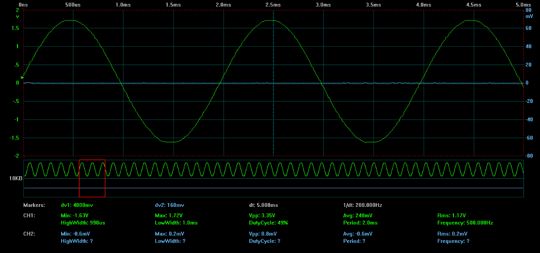
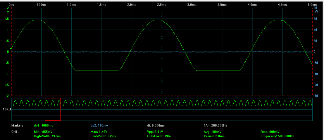
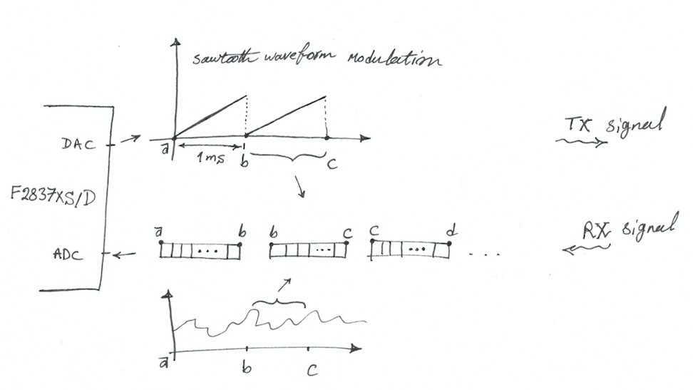
For my application, I need to generate ramp signal waveform with a DAC port and in the other hand, sampling the received signal at the same time with ADC port.

Please tell me your ideas and if any sample code is available for that?

Thanks for your help.

Best regards,

Amin

  • Hi Amin,

    I think you probably want to look at using an ePWM module as a timebase for updating the DAC via DMA trigger. Build a table in RAM for your waveform, and then use the DMA to loop through it, writing each value in the table to the DAC. Depending on the length of the ePWM period, the DAC will cycle through the waveform slower or faster.

    You can then use also use an ePWM module as the timebase for sampling the ADC. The DAC can be updated faster than the ADC can be triggered, so you may need to be careful if you want to use the same timebase. If you need to use two ePWM modules, they can be synchronized if needed.

    A good starting place would probably be the "adc_soc_epwm" example project in ControlSUITE. Extend this to have the ePWM SOC event also trigger a DMA move to update the DAC based on a table in RAM. If you then want to have the DAC update faster than the ADC is sampled, you can extend the project further by adding a second ePWM module to drive the DMA->DAC.
  • Hi Devin Cottier,

    Thank you for your help, in the “adc_soc_epwm" project, when I connect the signal to pin A0, the stored signal at CCS graph is not complete and input signal changes.

    Input signal before connect to ADC pin A0:

    After connect to A0:

    Why?

    Thanks & best regards,

    Amin

  • Hi Amin,

    Is this a negative voltage? You need to keep the input signal in the range of VSSA to VDDA (typically 0V to 3.3V). If the signal is out of range, it will be clamped by the ESD diodes inside the ADC pin. If too much current flow through these diodes (2mA continuous or 20mA instantaneous) then the device may be damaged or destroyed.