This thread has been locked.

If you have a related question, please click the "Ask a related question" button in the top right corner. The newly created question will be automatically linked to this question.

TMS320F28377D: Unexpected PWM output with CBC trip with zero/low ramp reference value

Part Number: TMS320F28377D

I am working on implemented peak-current mode control. It's working well for the most part but I'm seeing an issue with low RAMPMAXREF values. I have cycle-by-cycle limiting with dead-time working using the analog comparators to trigger a Digital Compare event that then triggers a T1 event in the AQ block of the PWM.

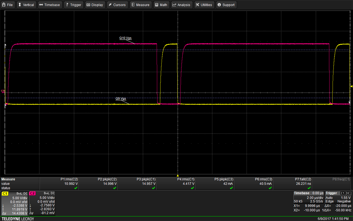
TBPRD = 999

CMPA = 500 (50% duty)

RAMPMAXREFS = 2000

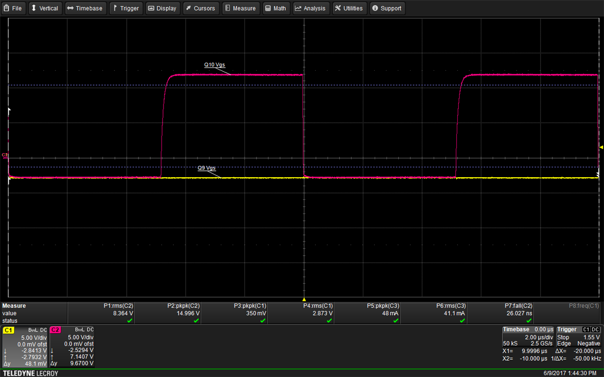
Yellow = PWM A

Pink = PWM B

Expected behavior, PWM A channel is cut off before CMPA would normally trigger it.


I'm having an issue when I set the RAMPMAXREFS to below a certain value, the gates behave unexpectedly.

RAMPMAXREFS = 0 (similar behavior up to around 450)


I would expect the analog comparator to trip instantly with a low RAMPMAXREFS and keep PWM A channel low and PWM B channel high. Instead I get this in-between behavior that looks like the comparator instantly trips for the PWM A channel but not the PWM B channel. Ocassionally the PWM B channel will stay low and the PWM A channel will output 50%. Certainly not a great situation.

Any ideas what is happening and how to resolve this? Any insight would be appreciated. Thank you!

  • Hi Noah,

    Do you see this behavior for all RAMPMAXREF values from 0 to 450 OR there are some values in this band that seem to work? Can you share your action qualifier (AQ) settings? I am assuming the high to low going edge of PWMA is a result of a trip-zone action, while the PWMB low to high going edge is the result of the T1 AQ event. Is this correct? Do you use slope compensation i.e. RAMPDECVAL?

    There are a few possible explanations here. We can narrow those down once I get the above information.

    Thanks.

    Hrishi

  • Hi Hrishi,

    Thanks for getting in touch.

    I'm not seeing any expected behavior in that 0 to 450 band. The upper end of RAMPMAXREF where normal behavior returns varies a bit, however. I am using ramp compensation though I haven't seeing any change in behavior if I set the RAMPDECVAL = 0.

    Here's my AQ settings.

    EPwm6Regs.AQCTLA.bit.ZRO = 0x2;       // Set PWMxA on CTR=Zero
    EPwm6Regs.AQCTLA.bit.CAU = 0x1;       // Clear PWMxA on event A, up count
    EPwm6Regs.AQTSRCSEL.bit.T1SEL = 0x1;  // configure DCA_EVT1 as trigger for T1 event
    EPwm6Regs.AQCTLA2.bit.T1U = 0x1;      // T1 event triggers PWM6A to go low

    My goal is to have PWMA set at ZERO and then CLEAR at T1 AQ event or CTR=CMPA. PWMB would then be the complimentary with some dead-time inserted. I did have this working across the board using the Digital Compare event but then realized that it manipulated the PWM signals after the Dead Band functionality.

    Here is my entire PWM/comparator setup too in case that helps clarify anything.


    // Configure EPwm6 for synchronous buck 
    //----------------------------------------------------------------
    
    EALLOW;
    // Configure GPIO10 and GPIO11 for ePWM6A and ePWM6B (respectively)
    GpioCtrlRegs.GPAMUX1.bit.GPIO10 = 1;    // 0=GPIO,  1=EPWM6A,  2=CANRXB(I),  3=ADCSOCBO(O)
    GpioCtrlRegs.GPAMUX1.bit.GPIO11 = 1;    // 0=GPIO,  1=EPWM6B,  2=SCIRXDB(I),  3=OUTPUTXBAR7
    GpioCtrlRegs.GPAPUD.bit.GPIO10 = 1;     // Disable pull-up on GPIO10 (EPWM6A)
    GpioCtrlRegs.GPAPUD.bit.GPIO11 = 1;     // Disable pull-up on GPIO11 (EPWM6B)
    
    //assign EPWM6 to CPU1
    DevCfgRegs.CPUSEL0.bit.EPWM6 = 0;
    
    // End protected registers
    EDIS;
    
    EPwm6Regs.TBCTL.bit.PRDLD = 0;
    
    // Period = u32PwmPeriodTicksIn-1 TBCLK counts
    EPwm6Regs.TBPRD = 999;
    
    //  Phase register
    EPwm6Regs.TBPHS.all = 0; // Set Phase register to zero
    
    // Counter mode:
    // TB_COUNT_UP:        Asymmetrical mode
    // TB_COUNT_DOWN:      Asymmetrical mode
    // TB_COUNT_UPDOWN:    Symmetrical mode
    EPwm6Regs.TBCTL.bit.CTRMODE = 0;
    
    // TB_DISABLE:         Phase loading disabled
    EPwm6Regs.TBCTL.bit.PHSEN = 0;
    
    // TB_SYNC_DISABLE:    Output sync signal disconnected
    // (i.e. ePWMn+1 module will not be synced to the current, ePWMn, module)
    EPwm6Regs.TBCTL.bit.SYNCOSEL = 3;
    EPwm6Regs.TBCTL2.bit.SYNCOSELX = 0;
    
    // Don't divide the PWM clock from the sys clock
    EPwm6Regs.TBCTL.bit.HSPCLKDIV = 0;
    EPwm6Regs.TBCTL.bit.CLKDIV = 0;
    // Free run TB module when stopped in debut mode
    EPwm6Regs.TBCTL.bit.FREE_SOFT = 0x3;
    
    // Clear timer counter
    EPwm6Regs.TBCTR = 0x0000;
    
    // Load new compare value when counter == period
    EPwm6Regs.CMPCTL.bit.LOADAMODE = 1; // load on CTR=PRD
    // Use shadow register when updating compare register
    EPwm6Regs.CMPCTL.bit.SHDWAMODE = 0;
    
    EPwm6Regs.AQCTLA.bit.ZRO = 0x2;       // Set PWMxA on CTR=Zero
    EPwm6Regs.AQCTLA.bit.CAU = 0x1;       // Clear PWMxA on event A, up count
    EPwm6Regs.AQTSRCSEL.bit.T1SEL = 0x1;  // configure DCA_EVT1 as trigger for T1 event
    EPwm6Regs.AQCTLA2.bit.T1U = 0x1;      // T1 event triggers PWM6A to go low
    
    // Enable writing to protected registers
    EALLOW;
    
    // Initialize HRPWM extension
    EPwm6Regs.CMPA.bit.CMPAHR = (1 << 8);
    
    // Reset HRPWM config register
    EPwm6Regs.HRCNFG.all = 0;
    
    // Enabled MEP control on:
    // HR_REP: Rising edge
    // HR_FEP: Falling edge
    // HR_BEP: Both rising and falling edges (useful for phase shift topologies)
    EPwm6Regs.HRCNFG.bit.EDGMODE = 2;
    
    // CMPAHR controls the MEP (Period mode)
    EPwm6Regs.HRCNFG.bit.CTLMODE = 0;
    
    // Shadow load on CTR=period
    EPwm6Regs.HRCNFG.bit.HRLOAD  = 1;
    
    #if (AUTOCONVERT)
      // Configure hardware to auto-convert duty-cycle/period/phase
      EPwm6Regs.HRCNFG.bit.AUTOCONV = 1;
    #endif
    
    // Turn on high-resolution period control
    EPwm6Regs.HRPCTL.bit.HRPE = 1;
    
    // Sync for high resolution period
    EPwm6Regs.TBCTL.bit.SWFSYNC = 1;
    
    // Disable writing to protected registers
    EDIS;
    
    #if (AUTOCONVERT)
    // Calling SFO() updates the HRMSTEP register with calibrated MEP_ScaleFactor.
    // MEP_ScaleFactor/HRMSTEP must be filled with calibrated value.
    u16SfoStatus = SFO_INCOMPLETE;
    
    // Call until complete
    while ( u16SfoStatus == SFO_INCOMPLETE )
    {
      // Check status of SFO update
      u16SfoStatus = SFO();
      if ( u16SfoStatus == SFO_ERROR )
      {
        // SFO function returns 2 if an error occurs & # of MEP steps/coarse step
        // exceeds maximum of 255.
        ESTOP0;
      }
    }
    #endif
     
    EPwm6Regs.CMPA.all = 0;
    
    EPwm6Regs.TBPHS.bit.TBPHS = 0;
    
    // enable or disable loading of a PWM module's phase register into time-base coutner
    // (introduce delay of u16PwmPhaseTicksIn)
    EPwm6Regs.TBCTL.bit.PHSEN =  0;
    
    // configure sync signal output select
    EPwm6Regs.TBCTL.bit.SYNCOSEL = 1;
    
    // Enable/disable high-resolution phase
    EALLOW;
    EPwm6Regs.HRPCTL.bit.TBPHSHRLOADE = 0;
    
    // TBPHSHR controls the MEP (Phase mode), default to period otherwise
    EPwm6Regs.HRCNFG.bit.CTLMODE = 0;
    
    
    EPwm6Regs.TZSEL.bit.DCBEVT1 = 1;
    
    // Configure PWM channel action when trip zone triggered
    EPwm6Regs.TZCTL.bit.TZA = 2;
    EPwm6Regs.TZCTL.bit.TZB = 2;
    EDIS;
    
    // Enable and configure dead-band module
    EPwm6Regs.DBCTL.bit.OUT_MODE = 3;
    
    // Enable and configure dead-band module
    EPwm6Regs.DBCTL.bit.IN_MODE = 0;
    
    // A and B channel polarity
    EPwm6Regs.DBCTL.bit.POLSEL = 2;
    
    // Configure falling- and rising-edge delay in TBCLK units
    EPwm6Regs.DBFED.bit.DBFED = 20;
    EPwm6Regs.DBRED.bit.DBRED = 20;
    
    // Enable SOC on A group
    EPwm6Regs.ETSEL.bit.SOCAEN = 1;
    // Config start of conversion select
    EPwm6Regs.ETSEL.bit.SOCASEL = 4;
    // Configure event for SOC Period select
    EPwm6Regs.ETPS.bit.SOCAPRD = 1;
    
    // Enable protected-mode registers
    EALLOW;
    
    // Select Digital Compare event to cause a trip zone event
    // DCxEVT2/Event 2 signifies cycle-by-cycle event
    EPwm6Regs.TZDCSEL.bit.DCAEVT2 = 2;
    // Select Digital Compare high event from TRIP4IN
    EPwm6Regs.DCTRIPSEL.bit.DCAHCOMPSEL = 3;
    
    // Use filtered or un-filtered event (i.e. apply blanking window logic)
    EPwm6Regs.DCACTL.bit.EVT2SRCSEL = 0;
    
    // Configure synchronous or asynchronous trigger
    EPwm6Regs.DCACTL.bit.EVT2FRCSYNCSEL = 1;
    
    // Filter block signal source
    EPwm6Regs.DCFCTL.bit.SRCSEL = 1;
    
    // Time-base counter equal to period (TBCTR = TBPRD) or 0 (TBCTR = 0)
    EPwm6Regs.DCFCTL.bit.PULSESEL = 1;
    
    // Configure blanking
    // Filter block use normal or inverted blanking window polarity
    EPwm6Regs.DCFCTL.bit.BLANKINV = 0;
    // Filter block Enable/Disable Blanking window
    EPwm6Regs.DCFCTL.bit.BLANKE = 1;
    
    // Disable protected-mode registers
    EDIS;
    
    // Filter block blanking window length
    EPwm6Regs.DCFWINDOW = 0;
    // Fliter block blanking window offset (then blanking window begins)
    EPwm6Regs.DCFOFFSET = 0;
    
    // connect comparator 3 high out to tripin4 via ePWM X-bar (mux 4 = 0)
    EALLOW;
    EPwmXbarRegs.TRIP4MUX0TO15CFG.bit.MUX4 = 0;
    EPwmXbarRegs.TRIP4MUXENABLE.bit.MUX4 = 1;
    EDIS;
    
    
    //----------------------------------------------------------------
    // Configure comparator
    //----------------------------------------------------------------
    
    EALLOW;
    
    //ADC A
    CpuSysRegs.PCLKCR14.bit.CMPSS3 = 0; //disble clock
    //assign CMPSS to CPU1
    DevCfgRegs.CPUSEL12.bit.CMPSS3 = 0;
    CpuSysRegs.PCLKCR14.bit.CMPSS3 = 1; //enable clock
    //Enable comparator and DAC logic?
    Cmpss3Regs.COMPCTL.bit.COMPDACE = eAdcCompEnableIn;
    
    //Configure the reference for DAC
    Cmpss3Regs.COMPDACCTL.bit.SELREF = 0;
    
    //Select synchronous or asynchronous comparator triggering
    Cmpss3Regs.COMPCTL.bit.ASYNCHEN = 1;
    
    //Invert comparator output?
    Cmpss3Regs.COMPCTL.bit.COMPHINV = 0;
    
    //Comparator High negative input connected to external pin or internal DAC?
    Cmpss3Regs.COMPCTL.bit.COMPHSOURCE = 0;
    
    
    //Configure Digital Filter
    //Maximum SAMPWIN value provides largest number of samples (5-bits)
    Cmpss3Regs.CTRIPHFILCTL.bit.SAMPWIN = 0x1F & 0x00;
    //Maximum THRESH value requires static value for entire window
    //(5-bits THRESH should be GREATER than half of SAMPWIN)
    Cmpss3Regs.CTRIPHFILCTL.bit.THRESH = 0x1F & 0x01;
    //Maximum CLKPRESCALE value provides the most time between samples (12-bits)
    Cmpss3Regs.CTRIPHFILCLKCTL.bit.CLKPRESCALE = 0x3FF & 0x001;
    
    //Reset filter logic & start filtering
    Cmpss3Regs.CTRIPHFILCTL.bit.FILINIT = 1;
    //Clear latch
    Cmpss3Regs.COMPSTSCLR.bit.HLATCHCLR = 1;
      
    //Configure CTRIPOUT path
    Cmpss3Regs.COMPCTL.bit.CTRIPHSEL = 0;
    
    //sync clear enable
    Cmpss3Regs.COMPSTSCLR.bit.HSYNCCLREN = 1;
    
    // Configure DAC and slope compensation
    // Clear DACVAL register before initial configuration
    Cmpss3Regs.DACHVALS.all = 0;
    Cmpss3Regs.DACLVALS.all = 0;
    Cmpss3Regs.DACHVALA.all = 0;
    Cmpss3Regs.DACLVALA.all = 0;
    Cmpss3Regs.RAMPMAXREFS = 0;
    Cmpss3Regs.RAMPMAXREFA = 0;
    
    // Emulation mode behavior, stop ramp immediately, after current ramp, or free-run?
    Cmpss3Regs.COMPDACCTL.bit.FREESOFT = 2;
    
    // Select to use DACVAL register or ramp for DAC source
    Cmpss3Regs.COMPDACCTL.bit.DACSOURCE = 1;
    
    // Select sync source for DAC ramp
    Cmpss3Regs.COMPDACCTL.bit.RAMPSOURCE = 5;
        
    // Load ramp from shadow or immediate?
    Cmpss3Regs.COMPDACCTL.bit.RAMPLOADSEL = 1;
    
    Cmpss3Regs.RAMPDECVALS = 7;
    // Disable protected-mode registers EDIS;

    From here I'd experiment with EPwm6.CMPA.bit.CMPA to 500 (50% max duty), the RAMPMAXREFS, and RAMPDECVALS via the debugger.

  • Noah,

    Thank you for sharing your configuration code. Seeing the same behavior for RAMPMAXREF from 0 to 450 is good. I believe this suggests that signal noise on the comparator input is enough to trip the PWM output at this low DAC level. 

    Now the question that needs to be answered is why PWMA output stays low while PWMB seems to be affected by the trip condition? I believe this is because of the deadband configuration. I think the DBRED is long enough that before the DBRED delay ends, the peak current signal trips the PWMA output and the output stays low. This trip maybe because of noise at that input. One way to get around this is to have a blanking window that starts from CTR = 0/1 and is at least equal to DBRED in length.

    The reason why PWMB seems okay is because it is derived as an inverted version of the PWMA action qualifier signal. The PWMA action qualifier signal seems to have a valid rising edge before it gets to the dead-band module. The deadband signal path for PWMB delays the falling edge of the PWMA signal, while the rising edge is not delayed by this signal path. As a result PWMB seems okay, even though PWMA (output) is completely eaten up the the DBRED path.

    Try generating PWMB using action qualifier settings for the PWMB output independently i.e. DBCTL[IN_MODE] = 0x2.

    BTW I notice that you have configured HR features as well. With peak current mode control, the duty cycle is decided by the time the feedback current hits the reference value. If you use the async trip path (to reset PWMA output), it will give you the best possible resolution. No need to enable HR features.

    I hope this helps.

    Hrishi

  • Hi Hrishi,

    Thank you for your response. I've been experimenting with various PWM settings such that the Action Qualifier block is setting the complementary PWM A/B signals and bypassing the DeadBand block and still getting the same undesired behavior. 

    EPwm6Regs.AQCTLA.bit.ZRO = 0x2;       // Set PWMxA on CTR=Zero
    EPwm6Regs.AQCTLA.bit.CAU = 0x1;       // Clear PWMxA on event A, up count
    EPwm6Regs.AQTSRCSEL.bit.T1SEL = 0x1;  // configure DCA_EVT1 as trigger for T1 event
    EPwm6Regs.AQCTLA2.bit.T1U = 0x1;      // T1 event triggers PWM6A to go low
    
    EPwm6Regs.AQCTLB.bit.PRD = 0x1;       // Clear PWMxB on CTR=PRD
    EPwm6Regs.AQCTLB.bit.CAU = 0x2;       // Set PWMxB on event A, up count
    EPwm6Regs.AQCTLB2.bit.T1U = 0x2;      // T1 event triggers PWM6B to go high
    
    EPwm6Regs.DBCTL.bit.OUT_MODE = 0x0;   // bypass dead-band module

    Values of RAMPMAXREFS closer to zero will cause PWM A channel to output CMPA duty, while PWM B channel is low. I can control whether it's PWM A or PWM B that is output by adjusting the blanking, so that could be a clue. I can add a blanking window offset to almost the period and then blank through CTR=Zero and get the behavior to remain on PWM B.

    Any other insights? I'll continue to play around.

    PS: Thank you for the reminder about the HRPWM. That is a remnant from when I was thinking of going with average current mode control.