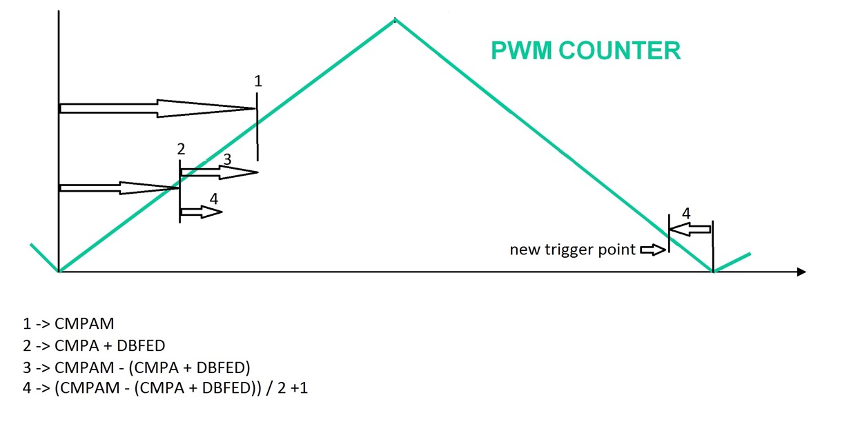
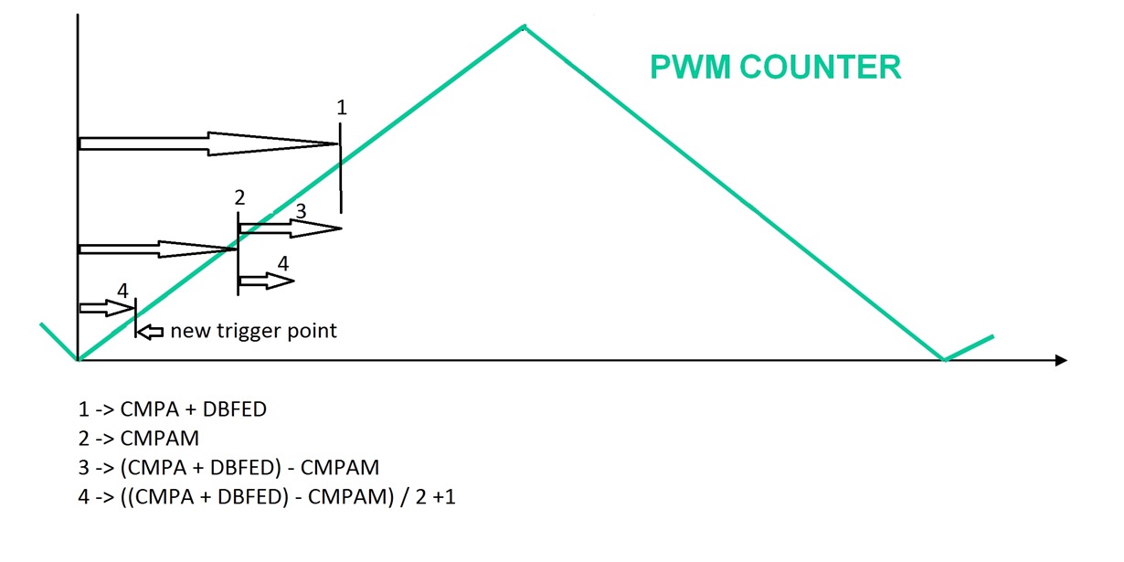
When calculating the next trigger point for the Start-of-Conversion in the MainISR, I'd like a couple clarifications on a couple of things. I've also reading the spruge9e-datasheet for the ePWM-module, but I'd still like a couple explanations.
Does the InstaSPIN library use center-aligned (dual edge) PWM pulse as a default?
Difference between CMPA (counter-compare A register) and CMPAM (counter-compare A register mirror)? Is it that CMPAM reads the currently active CMPA value, which is then updated to the earlier written CMPA value in HAL_writePwmData() when the counter = 0?
If shadow registers are enabled, then they act as a buffer register from which to load the new value to actual register at counter = 0? If shadow registers are disabled, then the new value written for example to CMPA takes effect immediately, possibly causing a glitch depending on the time of write?
Based on these I added some comments to explain the actions taken in HAL_setTrigger()
//! \brief     Set trigger point in the middle of the low side pulse
//! \param[in] handle    The hardware abstraction layer (HAL) handle
//! \param[in] ignoreShunt  The low side shunt that should be ignored
//! \param[in] midVolShunt  The middle length of output voltage
static inline void HAL_setTrigger(HAL_Handle handle,const SVGENCURRENT_IgnoreShunt_e ignoreShunt,
									const SVGENCURRENT_VmidShunt_e midVolShunt)
{
  HAL_Obj *obj = (HAL_Obj *)handle;

  PWM_Obj *pwm1 = (PWM_Obj *)obj->pwmHandle[PWM_Number_1];
  PWM_Obj *pwm2 = (PWM_Obj *)obj->pwmHandle[PWM_Number_2];
  PWM_Obj *pwm3 = (PWM_Obj *)obj->pwmHandle[PWM_Number_3];
  PWM_Obj *pwm;

  uint16_t nextPulse1 = (pwm1->CMPA + pwm1->CMPAM) / 2; // nextPulsex = ((to be written CMPA value, when counter = 0) + (currently active CMPA value)) / 2
  uint16_t nextPulse2 = (pwm2->CMPA + pwm2->CMPAM) / 2;
  uint16_t nextPulse3 = (pwm3->CMPA + pwm3->CMPAM) / 2;

  if(ignoreShunt == use_all) // if we can use all shunts, then figure out which ePWM-module has the shortest LOW-pulse and use that to set the time so all 3 outputs are LOW when we trigger ADC SoC?
    {
      if((nextPulse1 <= nextPulse2) && (nextPulse1 <= nextPulse3))
        {
          pwm = pwm1;
        }
      else if((nextPulse2 <= nextPulse1) && (nextPulse2 <= nextPulse3))
        {
          pwm = pwm2;
        }
      else
        {
          pwm = pwm3;
        }
    }
  else // if we can't use all 3 shunts, but only 2 at high duty cycles, then figure out again which ePWM-module to base the SoC timing
  {
	  if(midVolShunt == Vmid_a)
	  {
		  pwm = pwm1;
	  }
	  else if(midVolShunt == Vmid_b)
	  {
		  pwm = pwm2;
	  }
	  else
	  {
		  pwm = pwm3;
	  }
  }

  if(pwm->CMPAM >= (pwm->CMPA + pwm->DBFED))
  {
	  pwm1->CMPB = (pwm->CMPAM - (pwm->CMPA + pwm->DBFED)) / 2 + 1;  //Here I get a bit confused why are we using the CMPAM register if it holds (cont below.)
	  PWM_setSocAPulseSrc(obj->pwmHandle[PWM_Number_1],PWM_SocPulseSrc_CounterEqualCmpBDecr);  // the currently active CMPA to calculate the new trigger point for ADC SoC?
  }
  else
  {
	  pwm1->CMPB = ((pwm->CMPA + pwm->DBFED) - pwm->CMPAM ) / 2 + 1;
	  PWM_setSocAPulseSrc(obj->pwmHandle[PWM_Number_1],PWM_SocPulseSrc_CounterEqualCmpBIncr);
  }


