Other Parts Discussed in Thread: TMS320F28379D
Tool/software: Code Composer Studio
Hi,
I have made a code to generate three-phase PWM and H-bridge PWM signals, below is my code.
The three-phase PWM signals (EPWM 1 - 3) should be synchronized with each other and the H-bridge PWM signals (EPWM 4 - 5) should be synchronized with each other.
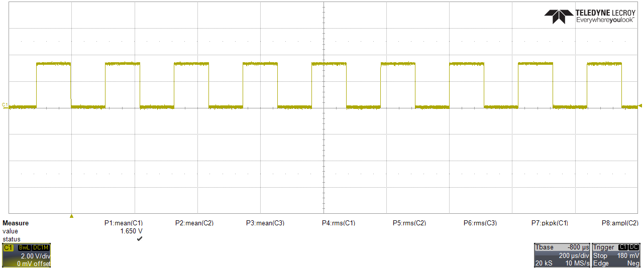
The three-phase PWM signals have a fundamental of 250 Hz and a switching frequency of 25 kHz.
The H-bridge PWM signals use phase-shift control and have a switching frequency of 100 kHz.
Now I have three questions:
(1) If I understand the datasheet of TMS320F28379D correctly, the System clock is 200 MHz. And the datasheet of TMS320F28379D also says that: For SYSCLK above 100 MHz, the EPWMCLK must be half of SYSCLKOUT, which means if SYSCLKOUT = 200 MHz, then the EPWM clock should be 100 MHz. However, if I set both of TBCTL.bit.HSPCLKDIV and TBCTL.bit.CLKDIV as 1, then will the EPWM clock be forced to be 200 MHz?
In addition, in my code, I set both of TBCTL.bit.HSPCLKDIV and TBCTL.bit.CLKDIV as 1, and if the EPWM clock actually is 100 MHz, and since I need 25 kHz switching frequency, the EPWM Period Register should be set to 100 [MHz] / 25 [kHz] / 2 = 2000 (up-down counting mode). However, it gives a switching frequency of 12.5 kHz, so I have to set the EPWM Period Register to be 1000 in order to get 25 kHz switching frequency. This is confusing for me. Why is it like this?
(2) I tried to update the three-phase duty-cycle in the EPWM1 ISR function generated at counter = zero. Every time the ISR function is called, a phase shift is added so that the voltage reference vector rotates at 250 Hz.
If I set EPwm1Regs.ETPS.bit.INTPRD = ET_3RD, which means to generate INT on every 3rd event, then the fundamental frequency is correct, 250 Hz, (every time the ISR is called, the voltage vector phase shift is 3 times than the previous correspondingly). However, if I decrease EPwm1Regs.ETPS.bit.INTPRD to ET_1ST, i.e. the interruption happens at each switching cycle, then the fundamental frequency becomes much lower.
However, if I keep EPwm1Regs.ETPS.bit.INTPRD to ET_1ST and decrease the switching frequency to 10 kHz, i.e. the interruption frequency also decreases to 10 kHz, then the fundamental becomes correct.
I thought that maybe this is because the interruption function is too time consuming for the DSP to process within one switching cycle so that some interruptions are lost in the meanwhile. However, I think the interruption function is not so long, and since the DSP works at 200 MHz and the interruption frequency is 25 kHz, which means 8000 calculation steps can be performed within one switching cycle, I think it should be far more than enough.
Any explanation and solution about this?
(3) The EPWM 4 and 5 are programmed based on the "TMS320x280x Enhanced Pulse Width Modulator (ePWM) Module Reference Guide (SPRU791)" Chapter 3.9 ZVSFB Converter. However, the EPWM4A and 5A are always giving 3.3 V whereas the EPWM4B and 5B are always giving 0 V. This is very confusing for me. Hope someone can explain to me.
Thank you very much!
//###########################################################################
//
// FILE: ePWM_five_channel.c
//
// Three-Phase SVPWM
// 25 kHz
// Phase A - EPWM1
// Phase B - EPWM2
// Phase C - EPWM3
//
// H-Bridge Phase-Shift
// 100 kHz
// Phase A - EPWM4
// Phase B - EPWM5
//
//###########################################################################
// Included Files
//
#include "F28x_Project.h"
#include "math.h"
//###########################################################################
// Defines
#define pi 3.141592653589793
#define two_pi 6.283185307179586
#define two_pi_over_three 2.094395102393195
#define sqrt_2 1.414213562373095
#define sqrt_3 1.732050807568877
//###########################################################################
// Global Variables
//
//%%%%%%%%%%%%%%%%%%%%%%%%%%%%%%%%%%%%%%%%%%%%%%%%%%%%%%%%%%%%%%%%%%%%%%%%%%%
// DC-Link Voltage
float32 u_dc = 48; // [V]
// Voltage Reference in Alpha-Beta Coordinate System
float32 u_ref_alpha; // [V]
float32 u_ref_beta; // [V]
float32 u_ref_angle; // [rad]
float32 u_ref_amp; // [rad]
//%%%%%%%%%%%%%%%%%%%%%%%%%%%%%%%%%%%%%%%%%%%%%%%%%%%%%%%%%%%%%%%%%%%%%%%%%%%
// Three-Phase Inverter PWM
float32 f_fundamental = 250; // [Hz]
float32 f_sw_three_phase = 25e3; // [Hz]
// Period: counting up and down
Uint16 N_three_phase_sw_period = 1000; // EPWM Period Register: N_three_phase_sw_period = 100 [MHz] / 25 [kHz] / 2 = 2000
// Dead Band
Uint16 N_three_phase_deadband = 25; // Dead Band Register: N_three_phase_deadband = 500 [ns] * 100 [MHz] /2 = 25
// PWM Reference Updating
Uint16 N_three_phase_update = 1; //
// PWM duty cycle: 1 means 100%
float32 duty_sw[3];
// Amplitude Modulation Index: 1 means 100%
float32 m_a = 0.9;
//%%%%%%%%%%%%%%%%%%%%%%%%%%%%%%%%%%%%%%%%%%%%%%%%%%%%%%%%%%%%%%%%%%%%%%%%%%%
// SinePWM or SVPWM ?
// 1: SinePWM
// 2: SinePWMTriangularInjection
// 3: SVPWM
Uint16 PWM_Algorithm = 3;
//%%%%%%%%%%%%%%%%%%%%%%%%%%%%%%%%%%%%%%%%%%%%%%%%%%%%%%%%%%%%%%%%%%%%%%%%%%%
// SinePWMTriangularInjection
float32 u_ref_abc_max,u_ref_abc_min;
float32 u_tri_ref; // triangular injection
//%%%%%%%%%%%%%%%%%%%%%%%%%%%%%%%%%%%%%%%%%%%%%%%%%%%%%%%%%%%%%%%%%%%%%%%%%%%
// SVPWM
Uint16 sector_SVPWM;
float32 duty_SVPWM[3];
float32 u_ref_amp_SVPWM;
float32 u_ref_ang_SVPWM;
float32 u_ref_alpha_SVPWM;
float32 u_ref_beta_SVPWM;
// SVPWM Table
// [section][a or b][states]
Uint16 V_SVPWM_basic[6][2][3] =
{
// sector 1
{
{1,0,0}, // Vector A: Phase A B C
{1,1,0} // Vector B: Phase A B C
},
// sector 2
{
{0,1,0}, // Vector A: Phase A B C
{1,1,0} // Vector B: Phase A B C
},
// sector 3
{
{0,1,0}, // Vector A: Phase A B C
{0,1,1} // Vector B: Phase A B C
},
// sector 4
{
{0,0,1}, // Vector A: Phase A B C
{0,1,1} // Vector B: Phase A B C
},
// sector 5
{
{0,0,1}, // Vector A: Phase A B C
{1,0,1} // Vector B: Phase A B C
},
// sector 6
{
{1,0,0}, // Vector A: Phase A B C
{1,0,1} // Vector B: Phase A B C
},
};
//%%%%%%%%%%%%%%%%%%%%%%%%%%%%%%%%%%%%%%%%%%%%%%%%%%%%%%%%%%%%%%%%%%%%%%%%%%%
// H-Bridge Inverter PWM
float32 f_sw_H_bridge = 100e3; // [Hz]
// Period: counting up
Uint16 N_H_bridge_sw_period = 500; // EPWM Period Register: N_H_bridge_period = 100 [MHz] / 100 [kHz] = 1000
// Duty Cycle
float32 duty_H_bridge = 0.5;
Uint16 N_H_bridge_duty;
// Dead Band
Uint16 N_H_bridge_deadband = 5; // Dead Band Register: N_three_phase_deadband = 100 [ns] * 100 [MHz] /2 = 5
//###########################################################################
// Function Prototypes
//
void InitEPwm1(void);
void InitEPwm2(void);
void InitEPwm3(void);
void InitEPwm4(void);
void InitEPwm5(void);
__interrupt void epwm1_isr(void);
// __interrupt void epwm2_isr(void);
// __interrupt void epwm3_isr(void);
// __interrupt void epwm4_isr(void);
// __interrupt void epwm5_isr(void);
void CurrentController(void);
void SinePWM(void);
void SVPWM(void);
void SinePWMTriangularInjection(void);
//###########################################################################
// Index
//
int16 i,j,k;
//
//
// Main
//
void main(void)
{
//
// Step 1. Initialize System Control:
// PLL, WatchDog, enable Peripheral Clocks
// This example function is found in the F2837xD_SysCtrl.c file.
//
InitSysCtrl();
//
// Step 2. Initialize GPIO:
// This example function is found in the F2837xD_Gpio.c file and
// illustrates how to set the GPIO to it's default state.
//
InitGpio();
//
// enable PWM1, PWM2, PWM3, PWM4, PWM5
//
CpuSysRegs.PCLKCR2.bit.EPWM1 = 1;
CpuSysRegs.PCLKCR2.bit.EPWM2 = 1;
CpuSysRegs.PCLKCR2.bit.EPWM3 = 1;
CpuSysRegs.PCLKCR2.bit.EPWM4 = 1;
CpuSysRegs.PCLKCR2.bit.EPWM5 = 1;
//
// For this case just init GPIO pins for ePWM1, ePWM2, ePWM3, ePWM4, ePWM5
// These functions are in the F2837xD_EPwm.c file
//
InitEPwm1Gpio();
InitEPwm2Gpio();
InitEPwm3Gpio();
InitEPwm4Gpio();
InitEPwm5Gpio();
//
// Step 3. Clear all interrupts and initialize PIE vector table:
// Disable CPU interrupts
//
DINT;
//
// Initialize the PIE control registers to their default state.
// The default state is all PIE interrupts disabled and flags
// are cleared.
// This function is found in the F2837xD_PieCtrl.c file.
//
InitPieCtrl();
//
// Disable CPU interrupts and clear all CPU interrupt flags:
//
IER = 0x0000;
IFR = 0x0000;
//
// Initialize the PIE vector table with pointers to the shell Interrupt
// Service Routines (ISR).
// This will populate the entire table, even if the interrupt
// is not used in this example. This is useful for debug purposes.
// The shell ISR routines are found in F2837xD_DefaultIsr.c.
// This function is found in F2837xD_PieVect.c.
//
InitPieVectTable();
//
// Interrupts that are used in this example are re-mapped to
// ISR functions found within this file.
//
EALLOW; // This is needed to write to EALLOW protected registers
PieVectTable.EPWM1_INT = &epwm1_isr;
EDIS; // This is needed to disable write to EALLOW protected registers
//
// For this example, only initialize the ePWM
//
EALLOW;
CpuSysRegs.PCLKCR0.bit.TBCLKSYNC = 0;
EDIS;
InitEPwm1();
InitEPwm2();
InitEPwm3();
InitEPwm4();
InitEPwm5();
EALLOW;
CpuSysRegs.PCLKCR0.bit.TBCLKSYNC = 1;
EDIS;
//
// Step 4. User specific code, enable interrupts:
//
//
// Enable CPU INT3 which is connected to EPWM1-3 INT:
//
IER |= M_INT3;
//
// Enable EPWM INTn in the PIE: Group 3 interrupt 1-3
//
PieCtrlRegs.PIEIER3.bit.INTx1 = 1;
//
// Enable global Interrupts and higher priority real-time debug events:
//
EINT; // Enable Global interrupt INTM
ERTM; // Enable Global real time interrupt DBGM
//
// Step 5. IDLE loop. Just sit and loop forever (optional):
//
for(;;)
{
asm (" NOP");
}
}
//
// InitEPwm1 - Initialize EPwm1 configuration
//
void InitEPwm1(void)
{
//
// Setup TBCLK
//
EPwm1Regs.TBCTL.bit.CTRMODE = TB_COUNT_UPDOWN; // Count up/down and down
EPwm1Regs.TBPRD = N_three_phase_sw_period; // Set timer period
EPwm1Regs.TBCTL.bit.PHSEN = TB_DISABLE; // Master Mode
EPwm1Regs.TBPHS.bit.TBPHS = 0x0000; // Phase is 0
EPwm1Regs.TBCTR = 0x0000; // Clear counter
EPwm1Regs.TBCTL.bit.HSPCLKDIV = TB_DIV1; // Clock ratio to SYSCLKOUT
EPwm1Regs.TBCTL.bit.CLKDIV = TB_DIV1;
EPwm1Regs.TBCTL.bit.PRDLD = TB_SHADOW; // No Active Loading
EPwm1Regs.TBCTL.bit.SYNCOSEL = TB_CTR_ZERO; // Sync down-stream
//
// Setup shadow register load on ZERO
//
EPwm1Regs.CMPCTL.bit.SHDWAMODE = CC_SHADOW;
EPwm1Regs.CMPCTL.bit.SHDWBMODE = CC_SHADOW;
EPwm1Regs.CMPCTL.bit.LOADAMODE = CC_CTR_ZERO;
EPwm1Regs.CMPCTL.bit.LOADBMODE = CC_CTR_ZERO;
//
// Set Compare values
//
EPwm1Regs.CMPA.bit.CMPA = duty_sw[0]; // Set Compare A Value
EPwm1Regs.CMPB.bit.CMPB = duty_sw[0]; // Set Compare B Value
//
// Set Actions
//
EPwm1Regs.AQCTLA.bit.CAU = AQ_SET; // Set Pwm1A on Event A during counting up
EPwm1Regs.AQCTLA.bit.CAD = AQ_CLEAR; // Clear Pwm1A on Event A during counting down
EPwm1Regs.AQCTLB.bit.CBU = AQ_CLEAR; // Clear Pwm1B on Event B during counting up
EPwm1Regs.AQCTLB.bit.CBD = AQ_SET; // Set Pwm1B on Event B during counting down
//
// Active high complementary PWMs - Setup the dead band
//
EPwm1Regs.DBCTL.bit.OUT_MODE = DB_FULL_ENABLE; // Fully-Enable: Enable both A and B
EPwm1Regs.DBCTL.bit.POLSEL = DB_ACTV_HIC; // Active High Complementary
EPwm1Regs.DBRED.bit.DBRED = N_three_phase_deadband; // Rising Edge High Complementary
EPwm1Regs.DBFED.bit.DBFED = N_three_phase_deadband; // Falling Edge High Complementary
//
// Interrupt where we will change the Compare Values
//
EPwm1Regs.ETSEL.bit.INTSEL = ET_CTR_ZERO; // Trigger INT on at Zero event
EPwm1Regs.ETSEL.bit.INTEN = 1; // Enable INT
EPwm1Regs.ETPS.bit.INTPRD = ET_3RD; // Generate INT on N'th event
}
//
// InitEPwm2 - Initialize EPwm2 configuration
//
void InitEPwm2(void)
{
//
// Setup TBCLK
//
EPwm2Regs.TBCTL.bit.CTRMODE = TB_COUNT_UPDOWN; // Count up/down and down
EPwm2Regs.TBPRD = N_three_phase_sw_period; // Set timer period
EPwm2Regs.TBCTL.bit.PHSEN = TB_ENABLE; // Slave Mode
EPwm2Regs.TBPHS.bit.TBPHS = 0x0000; // Phase is 0
EPwm2Regs.TBCTR = 0x0000; // Clear counter
EPwm2Regs.TBCTL.bit.HSPCLKDIV = TB_DIV1; // Clock ratio to SYSCLKOUT
EPwm2Regs.TBCTL.bit.CLKDIV = TB_DIV1;
EPwm2Regs.TBCTL.bit.PRDLD = TB_SHADOW; // No Active Loading
EPwm2Regs.TBCTL.bit.SYNCOSEL = TB_SYNC_IN; // Sync Flow-Through
//
// Setup shadow register load on ZERO
//
EPwm2Regs.CMPCTL.bit.SHDWAMODE = CC_SHADOW;
EPwm2Regs.CMPCTL.bit.SHDWBMODE = CC_SHADOW;
EPwm2Regs.CMPCTL.bit.LOADAMODE = CC_CTR_ZERO;
EPwm2Regs.CMPCTL.bit.LOADBMODE = CC_CTR_ZERO;
//
// Set Compare values
//
EPwm2Regs.CMPA.bit.CMPA = duty_sw[1]; // Set Compare A Value
EPwm2Regs.CMPB.bit.CMPB = duty_sw[1]; // Set Compare B Value
//
// Set Actions
//
EPwm2Regs.AQCTLA.bit.CAU = AQ_SET; // Set Pwm2A on Event A during counting up
EPwm2Regs.AQCTLA.bit.CAD = AQ_CLEAR; // Clear Pwm2A on Event A during counting down
EPwm2Regs.AQCTLB.bit.CBU = AQ_CLEAR; // Clear Pwm2B on Event B during counting up
EPwm2Regs.AQCTLB.bit.CBD = AQ_SET; // Set Pwm2B on Event B during counting down
//
// Active high complementary PWMs - Setup the dead band
//
EPwm2Regs.DBCTL.bit.OUT_MODE = DB_FULL_ENABLE; // Fully-Enable: Enable both A and B
EPwm2Regs.DBCTL.bit.POLSEL = DB_ACTV_HIC; // Active High Complementary
EPwm2Regs.DBRED.bit.DBRED = N_three_phase_deadband; // Rising Edge High Complementary
EPwm2Regs.DBFED.bit.DBFED = N_three_phase_deadband; // Falling Edge High Complementary
}
//
// InitEPwm3 - Initialize EPWM3 configuration
//
void InitEPwm3(void)
{
//
// Setup TBCLK
//
EPwm3Regs.TBCTL.bit.CTRMODE = TB_COUNT_UPDOWN; // Count up/down and down
EPwm3Regs.TBPRD = N_three_phase_sw_period; // Set timer period
EPwm3Regs.TBCTL.bit.PHSEN = TB_ENABLE; // Slave Mode
EPwm3Regs.TBPHS.bit.TBPHS = 0x0000; // Phase is 0
EPwm3Regs.TBCTR = 0x0000; // Clear counter
EPwm3Regs.TBCTL.bit.HSPCLKDIV = TB_DIV1; // Clock ratio to SYSCLKOUT
EPwm3Regs.TBCTL.bit.CLKDIV = TB_DIV1;
EPwm3Regs.TBCTL.bit.PRDLD = TB_SHADOW; // No Active Loading
EPwm3Regs.TBCTL.bit.SYNCOSEL = TB_SYNC_IN; // Sync Flow-Through
//
// Setup shadow register load on ZERO
//
EPwm3Regs.CMPCTL.bit.SHDWAMODE = CC_SHADOW;
EPwm3Regs.CMPCTL.bit.SHDWBMODE = CC_SHADOW;
EPwm3Regs.CMPCTL.bit.LOADAMODE = CC_CTR_ZERO;
EPwm3Regs.CMPCTL.bit.LOADBMODE = CC_CTR_ZERO;
//
// Set Compare values
//
EPwm3Regs.CMPA.bit.CMPA = duty_sw[2]; // Set Compare A Value
EPwm3Regs.CMPB.bit.CMPB = duty_sw[2]; // Set Compare B Value
//
// Set Actions
//
EPwm3Regs.AQCTLA.bit.CAU = AQ_SET; // Set PWM3A on Event A during counting up
EPwm3Regs.AQCTLA.bit.CAD = AQ_CLEAR; // Clear PWM3A on Event A during counting down
EPwm3Regs.AQCTLB.bit.CBU = AQ_CLEAR; // Clear PWM3B on Event B during counting up
EPwm3Regs.AQCTLB.bit.CBD = AQ_SET; // Set PWM3B on Event B during counting down
//
// Active high complementary PWMs - Setup the dead band
//
EPwm3Regs.DBCTL.bit.OUT_MODE = DB_FULL_ENABLE; // Fully-Enable: Enable both A and B
EPwm3Regs.DBCTL.bit.POLSEL = DB_ACTV_HIC; // Active High Complementary
EPwm3Regs.DBRED.bit.DBRED = N_three_phase_deadband; // Rising Edge High Complementary
EPwm3Regs.DBFED.bit.DBFED = N_three_phase_deadband; // Falling Edge High Complementary
}
//
// InitEPwm4 - Initialize EPWM4 configuration
//
void InitEPwm4(void)
{
//
// Setup TBCLK
//
EPwm4Regs.TBCTL.bit.CTRMODE = TB_COUNT_UP; // Count up
EPwm4Regs.TBPRD = N_H_bridge_sw_period; // Set timer period
EPwm4Regs.TBCTL.bit.PHSEN = TB_DISABLE; // Master Mode
EPwm4Regs.TBPHS.bit.TBPHS = 0x0000; // Phase is 0
EPwm4Regs.TBCTR = 0x0000; // Clear counter
EPwm4Regs.TBCTL.bit.HSPCLKDIV = TB_DIV1; // Clock ratio to SYSCLKOUT
EPwm4Regs.TBCTL.bit.CLKDIV = TB_DIV1;
EPwm4Regs.TBCTL.bit.PRDLD = TB_SHADOW; // No Active Loading
EPwm4Regs.TBCTL.bit.SYNCOSEL = TB_CTR_ZERO; // Sync down-stream
//
// Setup shadow register load on ZERO
//
EPwm4Regs.CMPCTL.bit.SHDWAMODE = CC_SHADOW;
EPwm4Regs.CMPCTL.bit.SHDWBMODE = CC_SHADOW;
EPwm4Regs.CMPCTL.bit.LOADAMODE = CC_CTR_ZERO;
EPwm4Regs.CMPCTL.bit.LOADBMODE = CC_CTR_ZERO;
//
// Set Compare values
//
EPwm4Regs.CMPA.bit.CMPA = N_H_bridge_sw_period / 2; // Set Compare A Value
EPwm4Regs.CMPB.bit.CMPB = N_H_bridge_sw_period / 2; // Set Compare B Value
//
// Set Actions
//
EPwm4Regs.AQCTLA.bit.CAU = AQ_SET; // Set Pwm4A on Event A during counting up
EPwm4Regs.AQCTLA.bit.CAD = AQ_CLEAR; // Clear Pwm4A on Event A during counting down
EPwm4Regs.AQCTLB.bit.CBU = AQ_CLEAR; // Clear Pwm4B on Event B during counting up
EPwm4Regs.AQCTLB.bit.CBD = AQ_SET; // Set Pwm4B on Event B during counting down
//
// Active high complementary PWMs - Setup the dead band
//
EPwm4Regs.DBCTL.bit.OUT_MODE = DB_FULL_ENABLE; // Fully-Enable: Enable both A and B
EPwm4Regs.DBCTL.bit.POLSEL = DB_ACTV_HIC; // Active High Complementary
EPwm4Regs.DBRED.bit.DBRED = N_H_bridge_deadband; // Rising Edge High Complementary
EPwm4Regs.DBFED.bit.DBFED = N_H_bridge_deadband; // Falling Edge High Complementary
}
//
// InitEPwm5 - Initialize EPWM5 configuration
//
void InitEPwm5(void)
{
//
// Setup TBCLK
//
EPwm5Regs.TBCTL.bit.CTRMODE = TB_COUNT_UP; // Count up
EPwm5Regs.TBPRD = N_H_bridge_sw_period; // Set timer period
EPwm5Regs.TBCTL.bit.PHSEN = TB_ENABLE; // Slave Mode
EPwm5Regs.TBPHS.bit.TBPHS = N_H_bridge_duty; // Phase is Shifted
EPwm5Regs.TBCTR = 0x0000; // Clear counter
EPwm5Regs.TBCTL.bit.HSPCLKDIV = TB_DIV1; // Clock ratio to SYSCLKOUT
EPwm5Regs.TBCTL.bit.CLKDIV = TB_DIV1;
EPwm5Regs.TBCTL.bit.PRDLD = TB_SHADOW; // No Active Loading
EPwm5Regs.TBCTL.bit.SYNCOSEL = TB_SYNC_IN; // Sync flow-through
//
// Setup shadow register load on ZERO
//
EPwm5Regs.CMPCTL.bit.SHDWAMODE = CC_SHADOW;
EPwm5Regs.CMPCTL.bit.SHDWBMODE = CC_SHADOW;
EPwm5Regs.CMPCTL.bit.LOADAMODE = CC_CTR_ZERO;
EPwm5Regs.CMPCTL.bit.LOADBMODE = CC_CTR_ZERO;
//
// Set Compare values
//
EPwm5Regs.CMPA.bit.CMPA = N_H_bridge_sw_period / 2; // Set Compare A Value
EPwm5Regs.CMPB.bit.CMPB = N_H_bridge_sw_period / 2; // Set Compare B Value
//
// Set Actions
//
EPwm5Regs.AQCTLA.bit.CAU = AQ_SET; // Set Pwm5A on Event A during counting up
EPwm5Regs.AQCTLA.bit.CAD = AQ_CLEAR; // Clear Pwm5A on Event A during counting down
EPwm5Regs.AQCTLB.bit.CBU = AQ_CLEAR; // Clear Pwm5B on Event B during counting up
EPwm5Regs.AQCTLB.bit.CBD = AQ_SET; // Set Pwm5B on Event B during counting down
//
// Active high complementary PWMs - Setup the dead band
//
EPwm5Regs.DBCTL.bit.OUT_MODE = DB_FULL_ENABLE; // Fully-Enable: Enable both A and B
EPwm5Regs.DBCTL.bit.POLSEL = DB_ACTV_HIC; // Active High Complementary
EPwm5Regs.DBRED.bit.DBRED = N_H_bridge_deadband; // Rising Edge High Complementary
EPwm5Regs.DBFED.bit.DBFED = N_H_bridge_deadband; // Falling Edge High Complementary
}
//
// epwm1_isr - EPWM1 ISR
//
__interrupt void epwm1_isr(void)
{
//=======================================================================
// Voltage Vector Calculation
CurrentController();
//=======================================================================
// Three-Phase PWM Calculation
switch(PWM_Algorithm)
{
case 1:
SinePWM();
break;
case 2:
SinePWMTriangularInjection();
break;
case 3:
SVPWM();
break;
}
//=======================================================================
// Three-Phase PWM Registers Update
N_three_phase_sw_period = round(100e6 / f_sw_three_phase / 4);
EPwm1Regs.TBPRD = N_three_phase_sw_period; // Set timer period
EPwm2Regs.TBPRD = N_three_phase_sw_period; // Set timer period
EPwm3Regs.TBPRD = N_three_phase_sw_period; // Set timer period
EPwm1Regs.CMPA.bit.CMPA = round(duty_sw[0] * N_three_phase_sw_period); // Set compare EPWM1 A value
EPwm2Regs.CMPA.bit.CMPA = round(duty_sw[1] * N_three_phase_sw_period); // Set compare EPWM2 A value
EPwm3Regs.CMPA.bit.CMPA = round(duty_sw[2] * N_three_phase_sw_period); // Set compare EPWM3 A value
//=======================================================================
// H-Bridge PWM Registers Update
N_H_bridge_sw_period = round(100e6 / f_sw_H_bridge / 2);
N_H_bridge_duty = round(duty_H_bridge * N_H_bridge_sw_period);
EPwm4Regs.TBPRD = N_H_bridge_sw_period; // Set timer period
EPwm5Regs.TBPRD = N_H_bridge_sw_period; // Set timer period
EPwm4Regs.CMPA.bit.CMPA = round(N_H_bridge_sw_period / 2); // Set Compare EPWM4 A Value
EPwm5Regs.CMPA.bit.CMPA = round(N_H_bridge_sw_period / 2); // Set Compare EPWM5 A Value
EPwm5Regs.TBPHS.bit.TBPHS = N_H_bridge_duty; // Phase Shift
//=======================================================================
// Clear INT flag for this timer
EPwm1Regs.ETCLR.bit.INT = 1;
// Acknowledge this interrupt to receive more interrupts from group 3
PieCtrlRegs.PIEACK.all = PIEACK_GROUP3;
}
void CurrentController(void)
{
u_ref_amp = u_dc / sqrt_3 * m_a;
N_three_phase_update = EPwm1Regs.ETPS.bit.INTPRD;
u_ref_angle = u_ref_angle + two_pi*f_fundamental/f_sw_three_phase * N_three_phase_update;
if(u_ref_angle > two_pi)
{
u_ref_angle = u_ref_angle - two_pi;
}
u_ref_alpha = u_ref_amp * cos(u_ref_angle);
u_ref_beta = u_ref_amp * sin(u_ref_angle);
}
void SinePWM(void)
{
duty_sw[0] = u_ref_alpha;
duty_sw[1] = - u_ref_alpha / 2 + sqrt_3 * u_ref_beta / 2;
duty_sw[2] = - u_ref_alpha / 2 - sqrt_3 * u_ref_beta / 2;
duty_sw[0] = duty_sw[0] * sqrt_3 / u_dc / 2 + 0.5;
duty_sw[1] = duty_sw[1] * sqrt_3 / u_dc / 2 + 0.5;
duty_sw[2] = duty_sw[2] * sqrt_3 / u_dc / 2 + 0.5;
}
void SinePWMTriangularInjection(void)
{
duty_sw[0] = u_ref_alpha;
duty_sw[1] = - u_ref_alpha / 2 + sqrt_3 * u_ref_beta / 2;
duty_sw[2] = - u_ref_alpha / 2 - sqrt_3 * u_ref_beta / 2;
u_ref_abc_max = duty_sw[0];
u_ref_abc_min = duty_sw[0];
for(i=1;i<=2;i++)
{
if(u_ref_abc_max < duty_sw[i])
{
u_ref_abc_max = duty_sw[i];
}
if(u_ref_abc_min > duty_sw[i])
{
u_ref_abc_min = duty_sw[i];
}
}
u_tri_ref = (u_ref_abc_max + u_ref_abc_min) / 2;
duty_sw[0] = (duty_sw[0] - u_tri_ref) * sqrt_3 / u_dc / 2 + 0.5;
duty_sw[1] = (duty_sw[1] - u_tri_ref) * sqrt_3 / u_dc / 2 + 0.5;
duty_sw[2] = (duty_sw[2] - u_tri_ref) * sqrt_3 / u_dc / 2 + 0.5;
}
//
void SVPWM(void)
{
// Note: u_ref is an amplitude-invariant space vector.
// per unit system
// The three-phase multi-level SVPWM output voltage
// is from -(N_level-1)/2*u_dc to (N_level-1)/2*u_dc,
// totally (N_level-1)*u_dc.
// Therefore, the voltage base should be (N_level-1)*u_dc/sqrt(3)
u_ref_amp_SVPWM = sqrt(u_ref_alpha*u_ref_alpha + u_ref_beta*u_ref_beta); // amplitude
u_ref_ang_SVPWM = atan2(u_ref_beta,u_ref_alpha); // angle
// sector detection & rotate or flip to Sector One
switch((int16)floor(u_ref_ang_SVPWM*3/pi))
{
// sector 1: [ 0 , pi/3 )
case 0:
sector_SVPWM = 1;
break;
// sector 2: [ pi/3 , pi*2/3 ): flip
case 1:
sector_SVPWM = 2;
u_ref_ang_SVPWM = two_pi_over_three - u_ref_ang_SVPWM;
break;
// sector 3: [ pi*2/3 , pi ): rotate
case 2:
sector_SVPWM = 3;
u_ref_ang_SVPWM -= two_pi_over_three;
break;
// sector 4: [ -pi , -pi*2/3 ) & pi: flip
case -3:
case 3:
sector_SVPWM = 4;
u_ref_ang_SVPWM = - two_pi_over_three - u_ref_ang_SVPWM;
break;
// sector 5: [ -pi*2/3 , pi/3 ) & pi: rotate
case -2:
sector_SVPWM = 5;
u_ref_ang_SVPWM += two_pi_over_three;
break;
// sector 6: [ -pi/3 , 0 ): flip
case -1:
sector_SVPWM = 6;
u_ref_ang_SVPWM = - u_ref_ang_SVPWM;
}
// too high voltage reference: convert over modulation to linear modulation
if(u_ref_amp_SVPWM * sqrt_3 / u_dc > 1)
u_ref_amp_SVPWM = sqrt_3 / 2;
else
u_ref_amp_SVPWM = 3 * u_ref_amp_SVPWM / 2 / u_dc;
// the 60-degree coordinate system
u_ref_alpha_SVPWM = u_ref_amp_SVPWM * cos(u_ref_ang_SVPWM);
u_ref_beta_SVPWM = u_ref_amp_SVPWM * sin(u_ref_ang_SVPWM);
//
duty_SVPWM[1] = u_ref_alpha_SVPWM - u_ref_beta_SVPWM / sqrt_3;
duty_SVPWM[2] = u_ref_beta_SVPWM * 2 / sqrt_3;
duty_SVPWM[0] = (1 - duty_SVPWM[1] - duty_SVPWM[2]) / 2;
// Vector_A * duty_cycle_Vector_A + Vector_B * duty_cycle_Vector_B + Vector_1_1_1 * duty_cycle_Vector_1_1_1
duty_sw[0] = V_SVPWM_basic[sector_SVPWM][0][0] * duty_SVPWM[1] + V_SVPWM_basic[sector_SVPWM][1][0] * duty_SVPWM[2] + duty_SVPWM[0];
duty_sw[1] = V_SVPWM_basic[sector_SVPWM][0][1] * duty_SVPWM[1] + V_SVPWM_basic[sector_SVPWM][1][1] * duty_SVPWM[2] + duty_SVPWM[0];
duty_sw[2] = V_SVPWM_basic[sector_SVPWM][0][2] * duty_SVPWM[1] + V_SVPWM_basic[sector_SVPWM][1][2] * duty_SVPWM[2] + duty_SVPWM[0];
}
//
// End of file
//