This thread has been locked.

If you have a related question, please click the "Ask a related question" button in the top right corner. The newly created question will be automatically linked to this question.

CCS/TMS320F28335: Issues with ezdsp-implemented closed loop contol - boost converter

Part Number: TMS320F28335

Tool/software: Code Composer Studio

Hello,

I think I need help with something. I am using ezdsp f28335 to implement closed loop integral control on a boost converter and I discovered that once the output reaches the reference, it waits for a second or two and continues to rise gradually up to about 13v and then starts to decrease until it crashes. I am boosting 3v to 8v. I have implemented the circuit using op-amps before so I know integral control is should be sufficient. I am using Ki = 5.

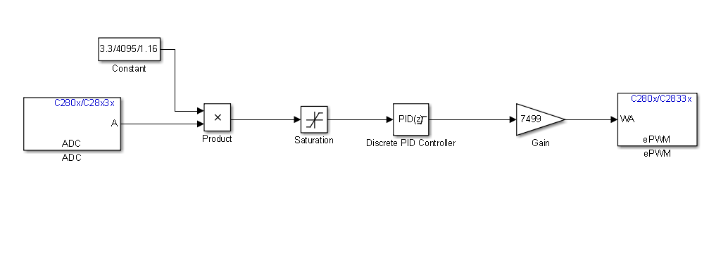
In the model below, I am feeding the error signal through the ADC to the PID controller. Ordinarily, as the duty cycle increases the error should approach zero and the duty cycle which is the output of the integrator should become constant but in my case when the error gets to zero the duty cycle doesn't stop increasing, it is as if -ve error is also causing an increase in duty cycle. This should not be!

Kindly advise me.

Thanks.

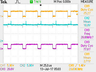
fig1 - epwm, output voltage, gate driver pulse

  • Hello,
    I am writing to let you know that a C2000 team member has been assigned to this post and should be answering shortly.

    Regards
    Baskaran
  • David,

    I see your other threads and I'm sorry to hear you are still in difficulty with this. I have already responded about discretizing the expected gain coefficients.

    Your model incorporates a PID controller with output saturation. Can you confirm you have implemented anti-windup? You should find it in the "PID Advanced" tab of the block properties.

    I would look carefully at the signals you are sampling, and at the input and output of the controller to see if there is some anomaly there. You can use a To workspace" blocks to export the variables to the Matlab workspace where they can be plotted. This may provide you with some clues.

    Also, since you are implementing an error junction externally, check the reference and feedback signals carefully on an oscilloscope. Look carefully at the setup of the ADC sampling and its' relationship with PWM timing. The sample point should be positioned well away from any PWM edges to avoid the influence of glitches there. In the C code, this is done in the PWM setup by assigning the ADC SOC to a suitable event in the timing pattern. There must be similar functionality in the Simulink block-set.

    BTW, I noticed in your latest post a rate transition block after the controller: what was that for?

    Apart from this, and based on the information you've provided, I regret I can't see anything which would prevent the control from working.

    Regards,

    Richard
  • Thanks Richard.

    1. The rate transition block is basically doing nothing per se. I guess now I know better.

    2. Anti-windup: I am using clamping and I am using a parallel discrete PID (forward euler).

    3. I have started working on the tips you gave me, now I am trying to figure out how to configure SCI Tx/Rx to plot the ADCRESULT into a scope or export it to workspace so I can know when and probably have an idea of where things are going wrong. The configuration is probably what I might need further tips on so I can see the problem and then think about tackling the problem. lol. Hopefully, I will get it solved today.

    Hope to hear from you soon.

    Kind regards.

    David.

  • Hi David,

    Thanks. Please let us know what you find. Good luck.

    Regards,

    Richard
  • Thanks Richard.

    I found my mistake. I didn't add an offset to the error signal, so as soon as the error hovers around zero and most especially when it becomes -ve, the mcu starts to misbehave. As soon as I added an offset, it starts to work fine. I completely forgot!!! **module8**

    However, I still have accuracy issues. I have recorded inaccuracies of up to -0.5v. This is the major problem I am battling with now. I even amplified the error signal to increase the SNB but I couldn't record much difference.

    I would appreciate:

    1. ideas on how to drastically improve the adc accuracy.

    2. tips/directions or maybe examples on how to monitor using MATLAB Simulink scope with SCI Tx/Rx . I have only been using ccs watch window thus far.

    Hope to hear from you soon.

    David.
  • Plus, I discovered that the error increased with decrease in reference voltage. it seems as it the 0.505v reference which I added to the error before sending it to the adc became bigger than its digital value which I subtracted from the adc output (ie. 0.5*TBPRD/3). *Up count*...

    In short with (0.5*7499/3 = 1250) offset, at about 10v reference I got an output voltage of 10 and sometimes 10.1 but when I reduced the reference to 6v, I was getting about 6.43v which is very bad. The offset's digital value appears to be changing. I don't know why!

    Moreover, the last 24 LSB's seems to be changing when I checked the 32 bit binary via CCS memory view, I believe by grounding ADCRESEXT via 22kohms and but grounding ADCREFM and ADCREFP via 2.2microFarad ceramic capacitor I would get reduced variations.

    I'd appreciate advise/pointers on these issues....

    Thanks.

    David
  • David,

    The action of the integrator is to drive the loop error to zero.  As long as there's a non-zero value entering the integral path, the output should be ramping one way or the other.  Can you take a close loop at what is happening in steady state at the integrator input?  You can check both the ADC input pin and the ADC result.

    BTW, how are you treating the ADC result?  Is it a signed number, and what is the range?

    The ADC has 12-bit resolution, so are you saying you represent it as a left justified 32-bit number?  If so, you are seeing just the bottom 4 bits changing because of noise.  Is that correct?

    Regards,

    Richard

  • Dear Richard,

    Thank you for your response.

    1. What I am doing is, I add 0.5v offset to the error signal (which I have previously divided by 10) before sending it into the ADC then I subtract the digital value of the offset from the output of the ADC before I feed the subsequent result into the integrator.

    2. I have set the output of the ADC to Unit16 (range 0 - 65535). And since I am using AdcRegs.ADCRESULT0 and not AdcMirror.ADCRESULT0 in order to have minimal wait states, the result is right shifted by 4 (i.e >>4).

    3. At steady state, I get an error of between 0.02 and 0.04 i.e about 0.48v enters the adc and this corresponds to 0.46v offset and 0.02v error. I don't know where I am losing 0.4v since I am supplying 0.5v as the dc offset and I am using a common ground for all supplies. Also, the value of AdcRegs.ADCRESULT0 from watch window is between 21300 & 21800(Uint16) and 0101010011100000 (binary) with the first 5msb's fixed and others changing. Also when I checked the memory location of (&AdcRegs.ADCRESULT0) and checking its 32 bit binary value I saw something like this (00000101110100000101010100000000) in which only the first 9 msb's were fixed, others were changing.

    Plus, the output I am getting is way off, sometimes I get errors of about 0.5v.

    One more thing, I discovered that if I vary the digital value of the offset accordingly (say if I am operating at a high duty cycle, If I decrease it to about 1200, I get better accuracy and if I am operating at a low duty cycle, If I increase it to about 1400, I also get better accuracy ). This makes me think the integrator is working but something goes wrong with the offset.

    I am a bit confused.

    David.

    *ccsv3.3*
  • David,

    Just want to make sure I understand.  Please can you confirm:

     - Your error signal after scaling, but before offset, is in the range -0.5 V to +0.5V.

     - You add +0.5 V offset, so the signal at the ADC input is 0 V to +1 V

     - The raw ADC result is in the range 0 to 65535 (since the ADCRESULT registers are left justified)

     - You are reading ~21800, which corresponds to about 1V of input (since the ADC range is 0 V to 3 V)

     - You say you right shift the result by 4 bits (why?)

    The ADCRESULT registers are 16-bit registers, not 32-bit.  If you perform a 32-bit read (how are you doing that?) you will probably be reading two register results concatenated.  ADCRESULT0 is even word aligned, so I think a 32-bit read returns that result in the low 16-bits and ADCRESULT1 in the high 16-bits.

    I don't think I completely understand what you're doing.  Can you confirm my understanding above please?  I feel I'm missing something.  Thanks.

    Regards,

    Richard

  • Thank you Richard.

    1. Yes. but more like - 0.5v to +0.75v.
    2. Yes. about 0v to +1.25v.
    3. Yes, I was getting above 20,000 decimal value.
    4. Correct. I think the 21800 doesn't make sense too because when I manually measure the signal entering the adc (i.e error + offset) I get about 0.5v.
    5. Maybe I didn't use the right term but what I mean is this AdcRegs.ADCRESULT0>>4, I guess I could have also used AdcMirror.ADCRESULT0; as this would require no shift. I got the info from the F2833X Analogue to Digital Converter Manual.
    6. 32 bit read. I got that through the CCSV3.3 by going to view->memory then I type &AdcRegs.ADCRESULT0 in the address window to see what's going on. And since I am converting just one signal I am not sure if there will be multiple result concatenation. But even with the 16 bit result which I got from the watch window, just the first 5 msb's are fixed.

    I am confused big time!

    David.
  • Hi David,

    Thank you for the information. I think you are facing at least two issues. To make progress I think you need to separate these and work on them one at a time.

    I see your separate forum thread on the ADC conversion issues. It would be prudent to resolve those first before moving forward with the system issues.

    Once we have reliable ADC data, the next step would be to look at what you're getting in steady state. From your description, zero loop error corresponds to 0.625 V at the ADC pin, which ends up after the right-shift as 0x2154 going into the controller. Full scale negative and positive is 0x0000 and 0x4208 respectively. You can check this with a voltage source at your ADC input. From that point things should start to come together.

    Regards,

    Richard

  • Yes Richard and i'd like to thank you for your patience.

    You are absolutely right, working with a messed up set of digital values is like trying to fetch water in a basket!

    Other professionals on here have also been trying to help me shed more light on my adc conversion palaver. I have two boards and I find it hard to believe both can be bad at the same time! I have run different tests, As I was advised by Tommy, I stepped back to try the ADC_SOC example. I converted adclo and I was getting between 0 and 20, well within acceptable limits but when I tried to convert 0.5v I got about 1500. I have removed all other connections to the board and I am only working with a grounded adclo and an RC filtered ADCINA (10ohms and 10pF). I have also opened the adcrefin since I am using internal reference. I don't know how to make the problem go away just yet.

    David.