


Part Number: TMS320F28377D
Other Parts Discussed in Thread: C2000WARE
Hi there,
I am trying to familiarize with the CLA for 28733D, and I was suggested to try the Lab9 in the document "C2000 Microcontroller Workshop, Revision 6.1, May 2015".
I did try to complete this exercise, and I would like to check whether what I have done is correct, since the exercise requires the user decide upon some inputs.
The tutorial says (on pag. 9-19, point # 6):
Edit Cla_9.c to implement the CLA operation as described in the objective for this lab exercise. Set RAMLS0, RAMLS1, RAMLS2, and RAMLS4 memory blocks as shared between the CPU and CLA. This is what I have done (on Cla_9.c):
//--- Memory Configuration - Master CPU and CLA Select
	MemCfgRegs.LSxMSEL.bit.MSEL_LS0 = 1;        // 0=CPU    1=CPU and CLA //Set RAMLS0, RAMLS1, RAMLS2, and RAMLS4
	MemCfgRegs.LSxMSEL.bit.MSEL_LS1 = 1;        // 0=CPU    1=CPU and CLA //memory blocks as shared between the CPU and CLA
	MemCfgRegs.LSxMSEL.bit.MSEL_LS2 = 1;        // 0=CPU    1=CPU and CLA
	MemCfgRegs.LSxMSEL.bit.MSEL_LS3 = 0;        // 0=CPU    1=CPU and CLA
	MemCfgRegs.LSxMSEL.bit.MSEL_LS4 = 1;        // 0=CPU    1=CPU and CLA
	MemCfgRegs.LSxMSEL.bit.MSEL_LS5 = 0;        // 0=CPU    1=CPU and CLA
Configure the RAMLS4 memory block to be mapped to CLA program memory space. Configure the RAMLS0, RAMLS1 and RAMLS2 memory blocks to be mapped to CLA data memory space. Note that the RAMLS0 memory block will be used for the CLA C compiler scratchpad.
//--- Memory Configuration - CLA Data Memory and CLA Program Memory Select
    MemCfgRegs.LSxCLAPGM.bit.CLAPGM_LS0 = 0;    // 0=CLA data memory    1=CLA program memory
    MemCfgRegs.LSxCLAPGM.bit.CLAPGM_LS1 = 0;    // 0=CLA data memory    1=CLA program memory
    MemCfgRegs.LSxCLAPGM.bit.CLAPGM_LS2 = 0;    // 0=CLA data memory    1=CLA program memory
    MemCfgRegs.LSxCLAPGM.bit.CLAPGM_LS3 = 0;    // 0=CLA data memory    1=CLA program memory
    MemCfgRegs.LSxCLAPGM.bit.CLAPGM_LS4 = 1;    // 0=CLA data memory    1=CLA program memory Config RAMLS4 memory block to be mapped to CLA program memory space
    MemCfgRegs.LSxCLAPGM.bit.CLAPGM_LS5 = 0;    // 0=CLA data memory    1=CLA program memory
Set Task 1 peripheral interrupt source to ADCAINT1 and set the other Task peripheral interrupt source inputs to “software” (i.e. none).
//--- Select Task interrupt source                     /******** TRIGGER SOURCE FOR EACH TASK (unlisted numbers are reserved) ********/
    DmaClaSrcSelRegs.CLA1TASKSRCSEL1.bit.TASK1 = 1;    // 0=none       8=ADCBINT3  16=ADCDINT1  32=XINT4     42=EPWM7INT   70=TINT2     78=ECAP4INT   95=SD1INT
                                                                                                   // 114=SPIRXINTC
    DmaClaSrcSelRegs.CLA1TASKSRCSEL1.bit.TASK2 = 0;    // 1=ADCAINT1   9=ADCBINT4  17=ADCDINT2  33=XINT5     43=EPWM8INT   71=MXEVTA    79=ECAP5INT   96=SD2INT
    DmaClaSrcSelRegs.CLA1TASKSRCSEL1.bit.TASK3 = 0;    // 2=ADCAINT2  10=ADCBEVT   18=ADCDINT3  36=EPWM1INT  44=EPWM9INT   72=MREVTA    80=ECAP6INT  107=UPP1INT
    DmaClaSrcSelRegs.CLA1TASKSRCSEL1.bit.TASK4 = 0;    // 3=ADCAINT3  11=ADCCINT1  19=ADCDINT4  37=EPWM2INT  45=EPWM10INT  73=MXEVTB    83=EQEP1INT  109=SPITXINTA
    DmaClaSrcSelRegs.CLA1TASKSRCSEL2.bit.TASK5 = 0;    // 4=ADCAINT4  12=ADCCINT2  20=ADCDEVT   38=EPWM3INT  46=EPWM11INT  74=MREVTB    84=EQEP2INT  110=SPIRXINTA
    DmaClaSrcSelRegs.CLA1TASKSRCSEL2.bit.TASK6 = 0;    // 5=ADCAEVT   13=ADCCINT3  29=XINT1     39=EPWM4INT  47=EPWM12INT  75=ECAP1INT  85=EQEP3INT  111=SPITXINTB
    DmaClaSrcSelRegs.CLA1TASKSRCSEL2.bit.TASK7 = 0;    // 6=ADCBINT1  14=ADCCINT4  30=XINT2     40=EPWM5INT  48=TINT0      76=ECAP2INT  87=HRCAP1INT 112=SPIRXINTB
    DmaClaSrcSelRegs.CLA1TASKSRCSEL2.bit.TASK8 = 0;    // 7=ADCBINT2  15=ADCCEVT   31=XINT3     41=
Enable CLA Task 1 interrupt. Enable the use of the IACK instruction to trigger a task,
//--- Enable use software to start a task (IACK)
    Cla1Regs.MCTL.bit.IACKE = 1;        // Enable IACKE to start task using software
//--- Enable CLA task interrupts

    Cla1Regs.MIER.bit.INT1 =1;         // Enable CLA interrupt 1 (and disable interrupt 8)
    asm(" EDIS");                      // Disable EALLOW protected register access
and then enable Task 8 interrupt.
//--- Force one-time initialization Task 8 - zero delay buffer
    Cla1Regs.MIER.bit.INT8 = 1;            // Enable CLA interrupt 8
    asm("  IACK  #0x0080");                // IACK - CLA task force instruction
    asm("  RPT #3 || NOP");                // Wait at least 4 cycles
    while(Cla1Regs.MIRUN.bit.INT8 == 1);   // Loop until task completes
In Main_9.c, I have commented out InitDma(); and added InitCla(); as per below:
void main(void)
{
//--- CPU Initialization
	InitSysCtrl();						// Initialize the CPU (FILE: SysCtrl.c)
	InitGpio();							// Initialize the shared GPIO pins (FILE: Gpio.c)
	InitXbar();							// Initialize the input, output & ePWM X-Bar (FILE: Xbar.c)
	InitPieCtrl();						// Initialize and enable the PIE (FILE: PieCtrl.c)
	InitWatchdog();						// Initialize the Watchdog Timer (FILE: WatchDog.c)

//--- Initialize CLA (Leo)
	InitCla();


//--- Peripheral Initialization
	InitAdca();							// Initialize the ADC-A (FILE: Adc.c)
	InitDacb();                                                     // Initialize the DAC-B (File: Dac.c)
	InitEPwm();							// Initialize the EPwm (FILE: EPwm.c)
	InitECap();							// Initialize the ECap (FILE: ECap.c)
//	InitDma();							// Initialize the DMA (FILE: Dma.c)
  ...
In Cla_9.c I have added the below code, in order to follow the instruction # 11 on pag. 9-20 (Modify the end of Cla_9.c to do the following:
- Enable the “CLA1_1” interrupt in the PIE (Hint: use the PieCtrlRegs structure)
- Enable the appropriate core interrupt in the IER register
)
//--- Enable the CLA interrupt

    EALLOW;
    IER |= M_INT11;   						// Enable CLA Task1 in PIE group #11
    PieCtrlRegs.PIEIER11.bit.INTx1 =1;      // Enable INT11 in IER to enable PIE group 11
    EDIS;

} // end of InitCla()
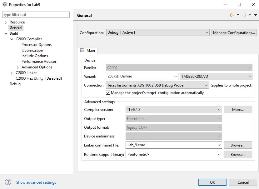
Moreover, this is the property window (I have used Lab_9.cmd in the "Linker command file" dropdown menu):
While this is the lists of files inside my project (is it correct to have both F2837xD_Headers_nonBIOS_cpu1.cmd and Lab_9.cmd ?):

When I build and debug Lab9 project, it looks like the CLA1 is disconnected

However, when I run the project, it looks like it is working, as the buffer AdcBufFiltered and AdcBuf keep updating:


And the graphs also seem to display the results properly:

The question is whether the code modifications I have reported above are correct, i.e. have I modified the code as the exercise required? and also, is it correct that CPU1_CLA1 displays as 'disconnected' in the debug window?
Thank you very much for your help.
Leo


