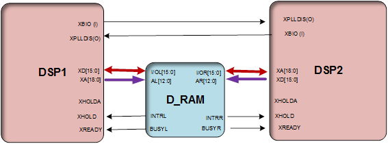
Pls review Our control Board schematic diagram:

I test total current about two DSP in our PCBA :
1.8V power, I_VDD(1.8V)+VDD1=359mA
3.3V power, I_ VDDIO(3.3V)+VDDA1/2/IO=156mA
It seemed that the power have exceed the IDDIO(30mA*2)+IDDA(40mA*2)=140mA, if the margin is not enough for 3.3V and 1.8V power in my design, pls note I design a common power supply 1.8V for VDD1 and VDD, 3.3V for VDDA1/2/IO and VDDIO, could you give some suggestion about DSP power margin design?and give some risk about my design DSP running speed.

