This thread has been locked.

If you have a related question, please click the "Ask a related question" button in the top right corner. The newly created question will be automatically linked to this question.

LAUNCHXL-F28377S: ADC Resolution Issue

Part Number: LAUNCHXL-F28377S
Other Parts Discussed in Thread: CONTROLSUITE, TMS320F28377S

Hello TI community,

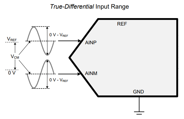
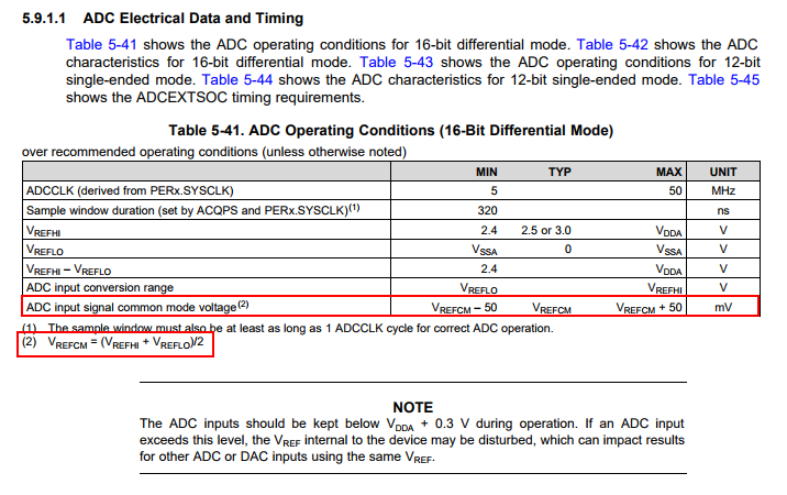
I am currently working on the LaunchXL-F28377S TI evaluation board. I am recently having issue with the ADC in 16-bit mode. I have my ADC configured to have SOC triggered from an ePWM. Currently I am using ADCINA2 and ADCINA3 where I have A3 pin grounded. I have a function generator connected for A2. I have an interrupt that is loading 256 samples into an array from the adc results register. In the past I was able to have up 3V of range before clipping (adc value of 65535). I am not sure what happened but I am only able to get up to 1.5V now into ADCINA2. I was wondering if anyone else has had this issue as well.

  • Hi Benden,

    The 16-bit ADC only functions in differential mode with a differential input voltage; you can't just ground the negative input.

    Do you get good results when you switch to 12-bit single-ended mode and sample pin A2?
  • Hello Devin,

    I am not sure why I can't ground the negative input. Wouldn't the differential simply subtract 0V from the positive input? I am trying to increase to the resolution of my of my ADC scans and was hoping I could take advantage of the 16 bits.
  • Hi Devin,

    I switch to 12 bit single ended mode and I still have clipping occurring.
  • Hi Brenden,

    This ADC uses a differential input voltage.  This is different than just subtracting the two pins.  With a truly differential input voltage both input change with respect to a common mode voltage:

    We specify that the input common mode should be within 50mV of the mid-point of the ADC conversion range:

    With the negative input connected to ground, the common mode specification will be violated (except when the positive input is close to max).  

    If your input signal is not natively differential, you will need to use an op-amp circuit to perform single-ended to differential conversion.  You can use either a single fully-differential op-amp or a pair of single-ended op-amps.   

  • For your clipping in 12-bit mode, are you sure that the function generator output is terminated correctly? If the termination is set to 50ohms but you don't terminate it you will get twice the voltage on the pin as you specify on the instrument. Have you verified the input voltage via DMM?
  • Hi Devin,

    I have confirmed using an oscilloscope that my function generator is operating as intended. I have the function generator set to sine wave, 2 kHz, low level of 200 mV and high level of 2V. The clipping occurs when my high level exceeds 1.5V.

    Also, I am a bit confused on what you mean by "termination" as well.

  • Hi Brenden,

    The next thing to check then would be the voltage on the VREFHI input. This should probably be 2.5V or 3.0V depending on the board.
  • On the LaunchXL board, both VREFHIA and VREFHIB are confirmed to be 3V using an oscilloscope. From the LaunchXL-F28377S schematics, VSSA and VREFLOB appear to be 0V as well. I have double checked that I configured the resolution of the ADC to be 12 bit single ended mode as well.
  • Also, strange thing is, to see if it was possibly my firmware was causing the issue, I flashed the example ADC program from controlSUITE. I was still running into the same issue though.
  • Hi Devin, I was also thinking if I connected a DC voltage source of 1.5V to the negative input, then theoretically, would I be able to then take advantage of the 16 bit resolution? With a positive input source properly biased to 1.5V as well of course.

  • Hi Brenden,

    If your VREFHI range is 0 to 3V and you start with 1.5V on both positive and negative inputs, this should give you a mid-scale conversion. If the positive input increases by 0.3V to 1.8V then the negative voltage would need to decrease by 0.3V to 1.2V. This will maintain the same common mode voltage of half the reference range: (1.8V + 1.2V)/2 = (1.5V + 1.5V)/2 = VREFHI/2.

    What is the impedance of your input and what is the S+H duration set to (S+H is controlled by the ACQPS field of the SOC configuration). If the S+H duration is too short for a given input impedance then you may have issues charging the ADC S+H capacitor during the S+H window, resulting in incorrect conversions.
  • Hello Devin,

    I am using code from the example adc_epwm source file. For 12-bit single ended signal mode, I am using acqps = 14, and for 16-bit mode I was using acqps = 63.

    Devin, in the data sheet is says that the common mode voltage for the inputs can not exceed 50 mV +/-. I was wondering what happens if it does? Are my conversion simply just not going to work, if so why?

    Also, this might be a dumb question but I was wondering for a particular situation. If I had my negative input at 1.5V DC and my positive input of a 3V DC signal, would I still be satisfying the common mode reference condition of 1.5V? My logic is that 3V signal is simply 1.5V common mode + 1.5V increase. In a sense I am also asking if my positive input was 0V DC (1.5V common mode - 1.5V) and my negative input be 1.5V DC.
  • Hi Brenden,

    You may want to confirm that your source is low impedance; acqps = 14 will give you the minimum possible S+H window, which will only be valid if you source is very low impedance and is using a high bandwidth driver. You can find additional guidance for calculating or simulating your external circuit by searching the e2e or by referring to the brief guidance in the TRM section "Choosing an Acquisition Window Duration"

    The ADC implementation in 16-bit mode is differential, so it needs a differential voltage. If you apply something else, we don't know what will come out of the ADC.
  • My sample acquisition time is set to 75 ns base off a 200 MHz system clock. My ADC is set 50 MHz with an ADC clock cycle of 20 ns.
  • Hi Brenden,

    The ADC input is not high impedance like a DMM or Scope. Instead it is a switched-capacitor circuit that needs to settle within whatever S+H time is allocated. The S+H time is configurable (via ACQPS field of the SOC configuration registers). You need to determine if the 75ns is appropriate for the impedance of whatever is driving your ADC input; higher impedance = longer S+H window to allow adequate time for input settling.

    An easy experiment to potentially rule out input settling issues is to increase the S+H duration significantly by writing the max possible value to the ACQPS field (511 I think).
  • Hello Devin,

    I just understood what you meant by input impedance, currently my function generator is has an output impedance of 50 ohms. If section 9.3.2 "Choosing an Acquisition Window Duration." There are variable Rs, Ron, and Ch that are mentioned. Would my 50 ohms or whatever I choose my input impedance be equivalent to Rs + Ron in this situation and I am not sure what Ch is as I can't find it in table 5-45 in the TMS320F28377S data sheet.
  • I set my sample and hold time acqps to the maximum S+H time, my adc reading still saturates..
  • Hello Devin,

    so I think I found what my problem is, for some reason, previously my oscilloscope confirmed that my voltage was within 0 to 3V but somehow something happened and function generator is producing twice the displayed voltage.

    Sorry for using so much of your time.
  • Hi Brenden,

    Glad that you were able to find the resolution.

    A function generator can produce twice the displayed voltage when the fgen output impedance is set to 50 ohms (this isn't always configurable - if it isn't configurable, assume that this is 50 ohms) but you don't use 50 ohm source termination at your input.