Part Number: TMS320F28035
Hi,
I want to confirm that my understanding about the IO pin state during reset is correct.
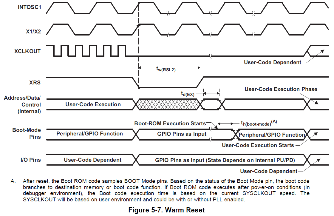
1. warm reset is all kinds of reset except for POR reset, right?
2. BOOT-MODE pins refer to boot mode select pins(GPIO34,37) and the pins used during boot loading. If the boot mode is SCI boot mode, the BOOT-MODE pins will include the RX and TX pins for code transfer, right?
3. "x" lines refer to that the state of INTOSC1, X1/X2 and IO pins are unknown?
4. during reset(XRS/ held low) the GPIO pins are as input(state depends on internal PU/PD), it can be found in the manual that
"The internal pullups on the pins that can be configured as ePWM outputs(GPIO0-
GPIO11) are all disabled asynchronously when the external reset signal (XRS) is low. The internal pullups
on all other pins are enabled on reset."
this is to prevent the PWM pins be high at the same time, right? But I'm confused that since it's input, why pull up circuit can still influence the voltage level on the pin? Can anyone tell me the difference when a GPIO is configured as an output or an input, at the circuit level?
5. BOR reset is not available in F2837x, F2807x and F28004x, so why don't we integrate BOR reset in the newer devices?

Figure 5-6 power-on reset