This thread has been locked.

If you have a related question, please click the "Ask a related question" button in the top right corner. The newly created question will be automatically linked to this question.

TMS320F28377S: TMS320F28377S ADC

Part Number: TMS320F28377S

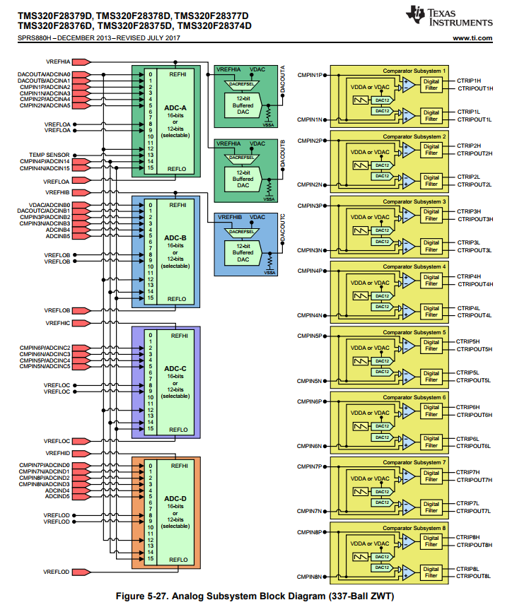
I don't understand the relationship between the input pins that go to each ADC and the figures that show only a few inputs hooked up to each of the 4 ADCs. To control a BLDC, I sense current on 2 of 3 phases; those signals are digitized and employed in a control algorithm; I also sense several other points for calibrating the ADC and diagnostics. In past designs, I used a F28335 to control 2 BLDCs. I want to use the F28377S to control 3 BLDCs, but it is not clear how I would use the 4 ADCs and how I would hook up the input pins. Can you give me some insights or point me to an example schematic?

  • Hi Timothy,

    Have a look at the diagram below.  The easiest way to think about the ADCs is as one ADC with 4 simultaneous S+H.  So if you want to sample 2 currents on 3 motors each you might use:

    ADCA: SOC0 samples A0 = MotorX, Phase 1 ; SOC1 samples A1 = MotorZ, Phase1 

    ABCB: SOC0 samples B0 = MotorX, Phase 2 ; SOC1 samples B1 = MotorZ, Phase2

    ADCC: SOC0 samples C2 = MotorY, Phase 1 ; SOC1 samples C3 = Blank or Cal/Diag

    ADCD: SOC0 samples D0 = MotorY, Phase 2 ; SOC1 samples D1 = Blank or Cal/Diag

    Additional channels can be used for additional cal or diag signals.

    A0, B0, C2, and D0 will all occur in parallel.  Note that there is no requirement to simultaneously sample the same channel numbers (e.g. A0/B0/C0/D0) unlike F28335 where you can simultaneously sample say A0/B0 or A3/B3 but can't simultaneously sample A0/B3.  


  • Hi Devin,

        Thanks very much for your response. I understand what you are saying, but I still don't understand why the chip would have 4 ADCs with multiple channels that are inaccessible. Plus why does the Vreflo occupy channels 8 and 9 on each ADC?

    Thanks,
    Tim

  • Hi Timothy,

    This is similar to not having GPIO0 to GPIO255 all pinned out; having more SW configurable channels than actual pins allows future designs to grow using the same architecture.

    The internal VREFLO connections can be used to self-calibrate the ADC offset error (this is not likely to be necessary on this device, since the offset error with factory trim is good). Another example of an internal-only connection is the temperature sensor. On older devices (e.g. F2803x family devices) these internal signals were muxed with an external channel and selection had to be done manually by SW. Now you can just configure an SOC for the target internal channel and use regular triggering to sample the internal channel.