


Other Parts Discussed in Thread: TMDSCNCD28069
Hello. everyone.
I have a question about HRPWM of TMS320F28069.
When PWM2 was operated by adding a phase difference to PWM1, In a phase difference, the output of PWM2 periodically becomes a skip cycle. *1
How can I get rid of the PWM2 output skip cycle?
* 1 Phase value at which skip occurs (EPwm2Regs.TBPHS.all)
0x00AE9800 to 0x00AEFF00
0x00AF2000 to 0x00AFFF00
0x00B02000 to 0x00B09700
Normal waveform
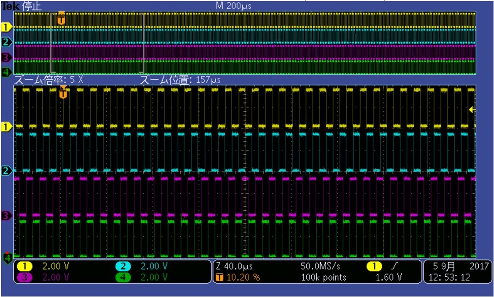
Yellow:PWM1A, Cyan:PWM1B, Magenta:PWM2A, Green:PWM2B
Illegal waveform
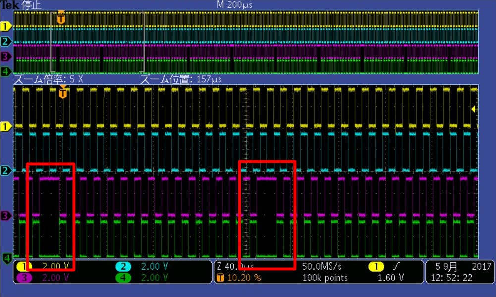
Yellow:PWM1A, Cyan:PWM1B, Magenta:PWM2A, Green:PWM2B
The project file can be sent immediately.
Best Regards,
Maekawa
