A related question is a question created from another question. When the related question is created, it will be automatically linked to the original question.
If you have a related question, please click the "Ask a related question" button in the top right corner. The newly created question will be automatically linked to this question.
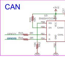
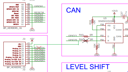
Is it possible that I remove R44 and connect a wire from GPIO70 to one position in J1-J8? For example I cut the PCB line of ADCIN14. Which line in the PCB is easier to cut? I don't need ADCs, DACs and PWM on chip and there are many posions in J1-J8 are not used. Or there are any better solutions?
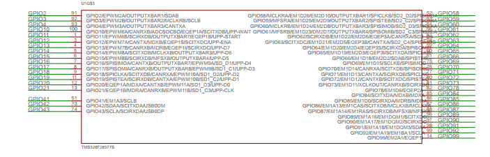
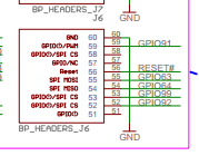
as for the discrepancy with GPIO92 and GPIO99, The BP_HEADERS_J6 schematic symbol has what the BoosterPack standard recommends. We try our best to align to this standard, but it is not always possible. You have correctly found that GPIO92 and GPIO99 do not have any SPI functionality muxed with them. Even though the BoosterPack Standard recommends that a Chip Select pin is available, we have at least provided a GPIO to manually control if needed.
As for resolving your issue, you can manually jump GPIO70 from R44 to any available location on the BoosterPack header dependent on your requirements. If you look at the same J6 header, Pin 58 can also be a SPI chip select signal. We have not connected any signal to that pin location so you are free to wire it up as you wish. It will not cause contention with any feature on the board.