Part Number: TMS320F28067
Hi,
One of my customers faced several F28067 ADC issues, during production, on different products, in these two months.
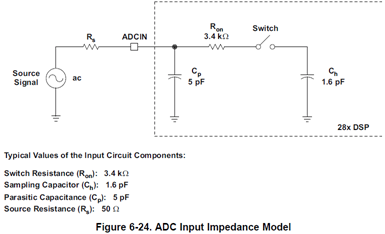
On their board, B0, B3 and B7 are connected to AGND. Between pin B0 and AGND, there's 1K resistor. B3 and B7 are connected together, with 10K resistor to AGND. B5 internally is connected to AGND, by register setting.
These three input channels are used for my own test. Here's the result.
1) ADC pin voltage: pin B0 is always 0 or 1mV. Pin B3 and B7, there's about 39mV. Where does it come from? Do we need to separate B3 and B7?
2) ADC offset calibration and accuracy. I did several test and found that:
2.1) ADC TRIM factory value from ROM is 0x0B, after sequential conversion, ADC result for B0 and B5 are 2 and 3 (these should be right); B3 is 0x6B; B7 is 0x4E. (These are wrong)
2.2) ADC TRIM is calibrated, with a new value 0x1EB, after sequential conversion, ADC result for B0 and B5 are always 0 (these should be wrong, although ADC result is 0. I tried to changed the TRIM by hand like 0x1FB or 0x08, B0 and B5 are still 0); B3 is 0x4C; B7 is 0x2E. 0x2E means 37mV, which is the real pin voltage 39mV.
2.1) and 2.2) are conflict. With different TRIM values, different channels are right, others are wrong.
3) ADC channel-to-channel variation: from test 2), we found the large variation of B3 and B7, although they are physically connected. If they are changed to different SOC, the result is more or less the same. Or B3's result is larger than B7's, or B7's is larger, or they are very close.
There are more then 15 pcs F28067, which have these issues.
Both internal and external reference are tried, the result are the same. Totally 15 SOCs. The ADC init code is check without any issues.
There's another case, on another about 5 pcs F28067.
All ADC results are good, except SOC8. If SOC8 are set with a larger sample time, from 7 to 10, the result can be good.
Br, Jordan