This thread has been locked.

If you have a related question, please click the "Ask a related question" button in the top right corner. The newly created question will be automatically linked to this question.

TMS320F28377S: TMS320F28377S PowerPad

Part Number: TMS320F28377S

Hello,

I am developing a PCB with TMS320F28377S (PTP 130 pins) and I have some doubts regarding the PowerPad.

Like for example:
- How many pads does PowerPad make?
- What is the distance between pads?
- Is it necessary to weld the PowerPad or can I put thermal paste / silicone film?
- Should the PowerPad be connected to the Ground of the PCB?

I await your response.

Best regards,
Carlos Martins

  • hwg_16c.zipCarlos,

    Please take a look at section 2.3 of attached document. To answer your specific questions:

    - How many pads does PowerPad make?  >> Many different variants of PowerPad exist inside many packages

    - What is the distance between pads? >> PowerPad is a single pad in the middle of the package to remove heat and provide ground - not sure I understand the question

    - Is it necessary to weld the PowerPad or can I put thermal paste / silicone film?  >> PowerPads must be soldered to the board pad to provide proper low thermal resistance and good grounding

    - Should the PowerPad be connected to the Ground of the PCB?  >>Depending on the device, most PowerPads are connected to internal Ground plane(s) through an array of thermal vias.

    Regards,

    Peter

  • Hi Peter,

    Thanks for your response.

    Sorry, I made a mistake in the question I asked.

    The question I wanted to ask would be:
    What is the distance between thermal paths?

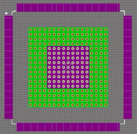
    At this time has the TMS320F28377SPTPS drawn according to two attached figures. In the figure "TMS320F28377SPTPS_1" has represented in the design of the microcontroller and PowerPad and the figure "TMS320F28377SPTPS_2" allows to differentiate the zone that can be soldered.

    These drawings were made according to the component datasheet information. As this information, regarding PowerPad, are not very enlightening, I have some doubts regarding the design.

    In your opinion, do you think I have something wrong with my drawing?

    I await your reply.

    Greetings,
    Carlos Martins

  • Hi Carlos,

    There is only one thermal pad inside the package, so the distance between thermal pads is confusing. Are you asking the distance between thermal pads of multiple MCU devices? Or maybe you are asking about the distance between thermal vias of the thermal pad? Please clarify, also please take a look at Figure 2-11 of the document I sent you in my last message.

    Your drawing looks OK, except maybe the solder mask opening for the thermal pad looks a little too large. It should be close to the size of the PowerPad.

    Regards,
    PEter
  • Hi Peter,

    Thanks for your response.
    I will consider your advice.

    Yes my question concerns the distance between thermal vias in the PowerPad.
    What is the distance between thermal vias? Will it be optional?

    Greetings,
    Carlos Martins

  • You may consider 0.3 mm (12 mils) diameter thermal vias, spaced about 2 mm appart,
    plated with 1 oz copper inside the barrel of each via. Using larger vias may wick too much solder from
    the themal pad. Using vias that are smaller than 0.2 mm (8 mils) reduces the amount of heat that can be
    removed from the package. The thermal vias used in the thermal land should not use the “wagon wheel”
    pads with spokes that are typically used for common vias. The thermal vias should use continuous
    connection around the hole diameter (instead of spokes) to achieve maximum heat removal. Smaller thermal land sizes and fewer vias may also be used and still attain a reasonable thermal
    transfer characteristics. The actual size of thermal lands and via patterns may be influenced by how much
    heat the processor is actually generating in a given application, and by how much room is needed to route
    signal traces underneath the footprint of the package. Other factors that influence heat dissipation include
    the thickness of copper plating and type of board material used. Filling vias with solder also helps getting the
    heat out of the IC leadframe, but it is and extra-cost option.

    Regards,
    Peter
  • Carlos,

    Also, for general information on PowerPad packages please take a look at these two documents:

    www.ti.com/.../slma002g.pdf
    www.ti.com/.../slma004b.pdf

    Regards,
    PEter