This thread has been locked.

If you have a related question, please click the "Ask a related question" button in the top right corner. The newly created question will be automatically linked to this question.

CCS/TMS320F28032: I don't quite understand how to implement the Code Security Module. Can someone answer my questions?

Part Number: TMS320F28032
Other Parts Discussed in Thread: C2000WARE, CONTROLSUITE

Tool/software: Code Composer Studio

Greetings,

I have been tasked with implementing the Code Security Module on our TMS320F28032 Chip. From reading about it I have a few questions in how I implement this. Here is what I think. I don't want to implement anything until I am certain this will not brick the chip up.

1. I have to go into the DSP2803x_SysCtrl.c and Change the CsmUnlock function to the password we want to use.

2. I have The code from the manuals 

void dspUnsecure (void)
{
    volatile int *CSM = (volatile int *)0x000AE0; //CSM register file
    volatile int *PWL = (volatile int *)0x003F7FF8; //Password location
    volatile int tmp;
    int I;
    // Read the 128-bits of the password locations (PWL)
    // in flash at address 0x3F 7FF8 - 0x3F 7FFF
    // If the device is secure, then the values read will
    // not actually be loaded into the temp variable, so
    // this is called a dummy read.
    for (I=0; I<8; I++) tmp = *PWL++;
    // If the password locations (PWL) are all = ones (0xFFFF),
    // then the device will now be unsecure. If the password
    // is not all ones (0xFFFF), then the code below is required
    // to unsecure the CSM.
    // Write the 128-bit password to the KEY registers
    // If this password matches that stored in the
    // PWL then the CSM will become unsecure. If it does not
    // match, then the device will remain secure.
    // An example password of:
    // 0x11112222333344445555666677778888 is used.
    EALLOW; // Key registers are EALLOW protected
    *CSM++ = 0x1111; // Register KEY0 at 0xAE0
    *CSM++ = 0x2222; // Register KEY1 at 0xAE1
    *CSM++ = 0x3333; // Register KEY2 at 0xAE2
    *CSM++ = 0x4444; // Register KEY3 at 0xAE3
    *CSM++ = 0x5555; // Register KEY4 at 0xAE4
    *CSM++ = 0x6666; // Register KEY5 at 0xAE5
    *CSM++ = 0x7777; // Register KEY6 at 0xAE6
    *CSM++ = 0x8888; // Register KEY7 at 0xAE7
    EDIS;


}

void dspSecure (void)
{
    volatile int *CSMSCR = 0x00AEF; //CSMSCR register
    //Set FORCESEC bit
    EALLOW; //CSMSCR register is EALLOW protected.
    *CSMSCR = 0x8000;
    EDIS;

}

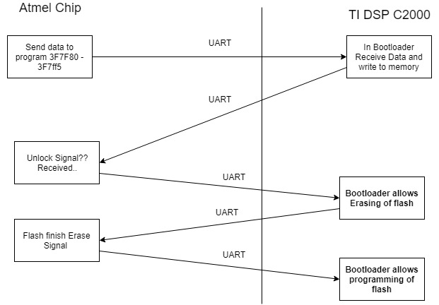
Once this implemented How do I go about unlocking and locking the chip. We are programming the device via UART from another chip which may throw an wrench into the system. Can someone explain to me the process of unlocking and locking the chip?

Thanks! 

  • Locking the chip involves programming a value other than all 1s in the password locations. If you are using c2000ware, you would input your passwords in the DSP2803x_CSMPasswords.asm file. Once you compile, link and program your project in flash, the device is secure from that point on.


    Unlocking (unsecuring) the device is explained in section 2.3.3 in page 28 of SPRUGL8C. Please point out to the specific step that is unclear.


    Since you are programming the flash via SCI, I presume you would be leveraging the SCI option in the on-chip boot-ROM. I suggest you flush this flow without passwords a few times and include the password only after ensuring the flow works as expected.

  • Hareesh,

    Thank you for the reply. I have the CSM.c and .h files in the design which look to do the same thing as the ASM file. their is a DSP unsecure function and a dsp secure function. 

    From what I understand from reading the SPRUGL8C document I need to change the registers in the DSP2803x_SysCtrl.c to a password.   I then compile and upload the code to the chip via UART. This works with an unsecured file. once this is uploaded I believe the chip is "locked" Now in order to unlock it do I need to upload new code with the DSPunsecure function in the beginning of the main function? or how do I go about unlocking this chip to upgrade the firmware?

    Thanks 

    Bill

  • You cannot upload new code without first unlocking the device. IOW, the flash must be unsecure first before you can even erase it. Unlocking or reprogramming the flash is fairly straightforward via JTAG. This can be enabled with a low-cost emulator like the XDS100 (http://processors.wiki.ti.com/index.php/XDS100 ). If using the JTAG is not an option and UART is the only option you could use, you still need to unlock the device first before running the flash API.

  • Hareesh,

    If I understand this correctly that re-flashing the chip via UART cannot utilize the CSM unlock because that feature is only available on Jtag. But using an jtag emulator will allow us to lock and unlock the chip via UART for re-flashing?

    Thank you

    Bill
  • Bill,

    You should be able to load a small piece of code (through UART) into un-secure memory which when run can unlock flash. Then you should be able to erase and re-program the flash.

    Regards,
    Manoj
  • Manoj,

    Great! Do you have any example code or information on how I might accomplish that? It is exactly what I need.

    Thanks

    Bill
  • Regardless of how you connect to the device (JTAG or UART), unlocking the device must happen before erase/program. And the code that unlocks the device may be transferred thru either conduits. If you use JTAG on an already locked part, ECSL may trip the connection to CCS. In this case, you may have to use the wait-boot mode in order to establish the JTAG connection. You can find the details in our docs. There are many posts that discuss this as well.

    p.s.: The code that unlocks is the same regardless of whether you use JTAG or SCI.

  • Bill,

    You already had this function "dspUnsecure". All you need to do in run this function from unsecure RAM after loading this small piece of code through UART.

    Regards,
    Manoj
  • Hareesh,

    Can you point me to the correct Document? I am having trouble finding it. Thanks
    Bill
  • Manoj,

    We have some memory that is being used as a bootloader. do I need to reset the processor and boot into the bootloader and run some code there? I'm sorry I am struggling to understand this. How do I run a specific part of code in a specific part of RAM?\

    Thanks

    Bill
  • Bill,

    Sorry, we don't any specific appnote / document which shows how it is done. But, have you already reviewed this example code

    C:\ti\controlSUITE\device_support\f2803x\v130\DSP2803x_examples_ccsv5\f2803x_flash_kernel

    Regards,
    Manoj
  • The datasheet (SPRS584), SPRUGL8 and SPRUGO0B have all the information you need. www.ti.com/.../sprabv4b.pdf is a good resource as well.
  • Manoj,

    When flashing via UART should I program address 0x33FFF8 with the correct password and then proceed with flash? Is this the correct way to use the CSM while programming from UART?

    Thanks 

    Bill

  • Bill,

    I would recommend you to first program flash and then proceed with programming flash passwords just to make sure you don't lock yourself in the middle of the programming process. This can happen if you get reset the device after programming the password.

    Regards,

    Manoj

  • Manoj,

    I can reliably program the flash but, are you saying I can still program the flash while the device is locked and THEN program the passcode to unlock it? Where do I program the passcode? Address?

    Thanks!

    Bill
  • You cannot erase/program the flash unless you unlock it first. As indicated in my first reply, If you are using c2000ware, you would input your passwords in the DSP2803x_CSMPasswords.asm file.

  • Okay, I am not sure if I have C200Ware, I think I do but path you are specifying I do not have. This is getting irritating I am really confused and I am getting 1 or two sentences back. I am new to this and I could really use your help. 

    1. I can program the chip vial UART. I send the hex file to the flash while in the bootloader which is installed in the factory. 

    2. I DO NOT know what to send first to unlock the chip I've asked this multiple times but have not received a response on how to do this. A phone call or anything I'll take 

    3. Below is what I have I cannot find  a control suite directory. I would really appreciate it if you sat down and helped me fix this.  Something like Step 1: do this, Then this, etc.

    Thank you

  • I still do not understand how to do this. Can someone please help? This issue is not solved and is delaying other things.

    Thanks

    Bill
  • Bill,

                I am at loss to understand exactly where you are stuck and where you need help. See if the below helps. If not, it may be more time-efficient to have a call. If one is needed, please work through the TI FAE supporting you to arrange one.


    It is important to differentiate the two steps, viz

    (i) How to add passwords to the project

    This is done by editing the DSP2803x_CSMPasswords.asm file in C:\ti\c2000\C2000Ware_1_00_02_00\device_support\f2803x\common\source, compiling & linking your project and burning it into flash. From this point on, the device is "secure" and must be "unsecured" before accessing any secure memory (RAM/Flash). This includes the erase/program operation for flash.


    (ii) How to unlock the device before the erase/program operation.

    You need to unlock the device first with the passwords before you will be allowed to access the flash. You will need to run the CsmUnlock() from unsecure memory. You can edit the linker command file to place any section of code into a desired memory.


    Program the COFF file with passwords via JTAG first, read the password locations and ensure the correct passwords are there before attempting programming via SCI.


    Here is the existing example code / documentation which can be used for this topic.


    Existing example code:

    I presume you are using c2000ware to develop your project. C2000ware is the preferred platform for code development and supersedes Controlsuite. If you do not have Controlsuite installed (which you can easily download from the TI website at www.ti.com/.../controlsuite , the equivalent path for controlSUITE\device_support\f2803x\v130\DSP2803x_examples_ccsv5\f2803x_flash_kernel is

    C:\ti\c2000\C2000Ware_1_00_02_00\device_support\f2803x\examples\c28\f2803x_flash_kernel


    Example code and document explaining how to invoke flash API function calls from BOOTROM.


    controlSUITE\libs\utilities\flash_api\2803x\v100a\doc (In c2000ware, it is C:\ti\c2000\C2000Ware_1_00_02_00\libraries\flash_api\f2803x\docs)

    controlSUITE\libs\utilities\flash_api\2803x\v100a\example_ccsv5 (In c2000ware, it is C:\ti\c2000\C2000Ware_1_00_02_00\libraries\flash_api\f2803x\example_ccsv5)

  • Hareesh,

    Thank you for the reply. Unfortunately the code in this chip was not started with C2000ware. I inherited it and understand most of it. I have c2000ware 1_00_01_00 which has the files you are describing. I am attaching a flow chart to help explain where I am coming from 

    The chip has a boot loader and an application loaded into it. The bootloader does not need to be secured and I was hoping that I could put the chip into bootloader mode by sending it a command via UART and then sending the CSM password via UART and the bootloader could load it to 0x 3F780 

    Once the password is loaded into the address will I then be able to load hex data into the flash? Here is a snapshot of the memory

    So that is where I am right now. Thank you so much for your help

    Bill

  • It is OK if your project was developed with Controlsuite. It is largely compatible with c2000ware.

    Exactly where is your bootloader placed?

    Address "0x3F780" does not appear to be correct. Did you mean the address of the KEY registers, AE0-AEF?

    I didn’t understand what you mean by "The bootloader does not need to be secured ". In this device, either the entire flash is secured or not. I also did not understand the flow diagram well. What does the box containing "Send data to program 3F7F80-3F7FF5" do? Understand our docs suggest these locations must be programmed to 0's if CSM is used, but how/why is it relevant to kickstart the flash programming process? Could you please add more precision to your flow diagram? Specifically, what data is exchanged between the two MCUs, where that data is stored and what action is initiated based on those data? IOW, the sequence from start-to-finish on how flash programming is initiated and completed. Understand you are looking for guidance on the unlocking part, but would like to get a fair understanding of the sequence you have in mind.
  • Hareesh,

    Thank you again for the reply. Here is where my bootloader is: 

    MEMORY
    {
    PAGE 0 :
       /* BEGIN is used for the "boot to SARAM" bootloader mode   */
    
       BEGIN      : origin = 0x000000, length = 0x000002
       RAMM0      : origin = 0x000050, length = 0x0003B0
       RAML0L1    : origin = 0x008000, length = 0x000C00
       RESET      : origin = 0x3FFFC0, length = 0x000002
       IQTABLES   : origin = 0x3FE000, length = 0x000B50     /* IQ Math Tables in Boot ROM */
       IQTABLES2  : origin = 0x3FEB50, length = 0x00008C     /* IQ Math Tables in Boot ROM */
       IQTABLES3  : origin = 0x3FEBDC, length = 0x0000AA	 /* IQ Math Tables in Boot ROM */
    
       BOOTROM    : origin = 0x3FF27C, length = 0x000D44
    
    
    PAGE 1 :
    
       BOOT_RSVD   : origin = 0x000002, length = 0x00004E     /* Part of M0, BOOT rom will use this for stack */
       RAMM1       : origin = 0x000480, length = 0x000380     /* on-chip RAM block M1 */
       RAML2       : origin = 0x008C00, length = 0x000400
       RAML3       : origin = 0x009000, length = 0x001000
    }

    The application code starts at 0x000880 and ends with the CSM at 0x3F7FF8 which lasts for 8 bytes.

    The Atmel micro controller sends a command to go into the boot loader and starts sending the application code to the boot loader which then places the data in the memory starting where the application code resides. A reset command is issued and the C2000 boots to application.  So largely the data shared between the two processors is hex image data.. 

    The only thing I am trying to do is prevent someone from hooking a JTAG to the device and lifting the code off of the flash in the C2000. I was hoping all I had to do is before the hex data is sent while the C2000 is in the boot loader is to send some data to the correct registers on the chip and unlock the device so I can send the rest of the data and the boot loader can place it in the correct location to run the application. If this does not help would you be open to a screen sharing session or a phone call?

    Thanks 

    Bill

  • Could you please post your entire linker command file (with the section allocation)? Yes, I am open for a call or a screen-sharing session.