This thread has been locked.

If you have a related question, please click the "Ask a related question" button in the top right corner. The newly created question will be automatically linked to this question.

LAUNCHXL-F28069M: Deadband for ePWM in Simulink

Part Number: LAUNCHXL-F28069M


Hi all! ;)

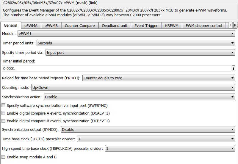
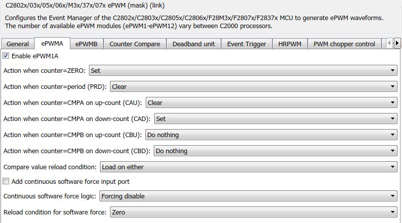
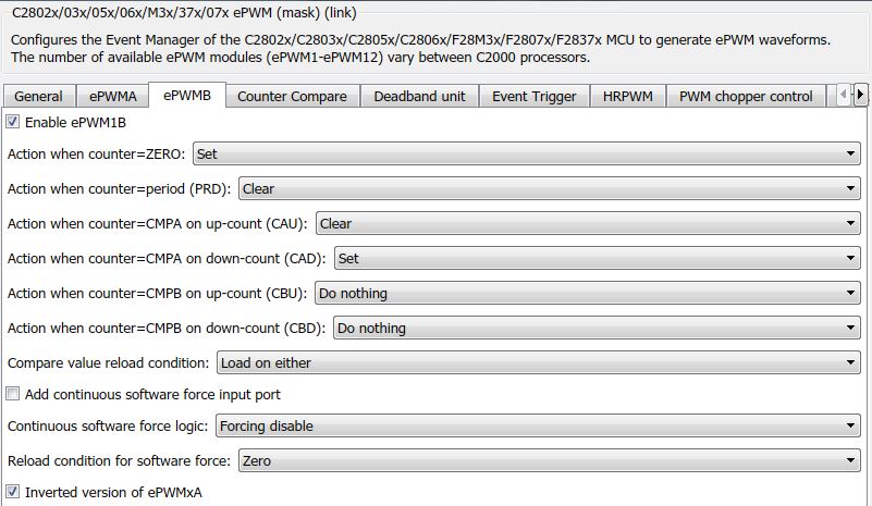
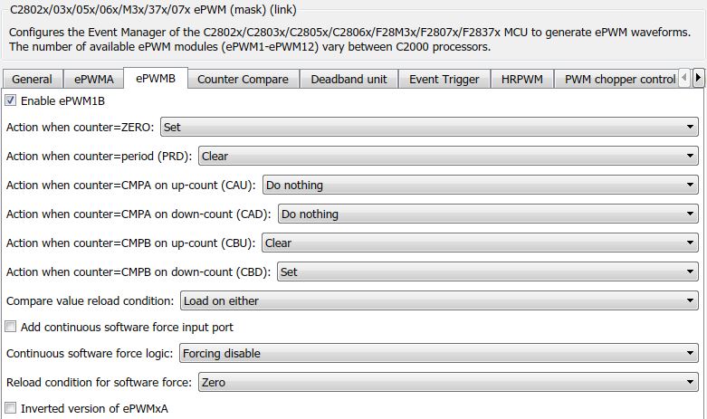
I have now finished the hardware work to build my own three-phase inverter for motor control. The inverter shall be run by my F28069M-LaunchPad. To avoid a shoot-through in the IGBT-module (B6 bridge topology) I wanted to insert a dead time between the falling edge and the next rising edge. I wanted the dead time to be 1.4 µs which is about 126 clock cycles on my 90 MHz MCU.
I found post here on the E2E forums that describes all the necessary steps to set such a dead time in the "Deadband unit" tab in Simulink:

https://e2e.ti.com/support/microcontrollers/c2000/f/171/p/152067/551099#551099

However, I set everything just like mentioned in this post but my oscilloscope shows that there is no deadband inserted between the falling edge of one switch and the rising edge of the other switch. Or let's better put it this way: The deadband of 1.4 µs is indeed inserted, but not only the rising edge is delayed, also the falling edge is delayed. (I found this out because at 10 % duty cycle the ePWM1A signal is constantly low and the ePWM1B signal is constantly high.) This should not happen. The falling edge should occur immediately and only the rising edge should be delayed.
Do you know what I did wrong here? I will attach some screenshots of my configuration below.

Best regards,
Armin

  • Hi Armin,

    Could you please post the code generated by simulink as well? One suggestion is to start debugging the code generated by simulink and look for mismatch between the C code and Simulink setting. Thanks!

    Best regards,
    Chen
  • Hi Armin,

    Please do mention the version of the MATLAB and TI C2000 support package you are using in this case.

    Regards,

    Venkatesh Chilapur

  • Hi Venkatesh,

    I am using MATLAB version 9.2.0.538062 (R2017a) and the TI C2000 Support Package version 17.1.2. And I have CCSv6 installed.

    Best regards,

    Armin

  • Hi Chen,

    I attached the generated code below (only the part that refers to the setup of the deadband unit, if I should upload more, just tell me).
    Do you see anything wrong at first sight? Can I find a detailed documentation of all the registers and settings that are mentioned in the C code in the Technical Reference Manual of the MCU (chapter about ePWM)?

    Best regards,
    Armin

    /*
     * File: TEST_end_ePWM_SCI.c
     *
     * Code generated for Simulink model 'TEST_end_ePWM_SCI'.
     *
     * Model version                  : 1.145
     * Simulink Coder version         : 8.12 (R2017a) 16-Feb-2017
     * C/C++ source code generated on : Tue Nov 14 14:20:57 2017
     *
     * Target selection: ert.tlc
     * Embedded hardware selection: Texas Instruments->C2000
     * Code generation objectives: Unspecified
     * Validation result: Not run
     */
    
    #include "TEST_end_ePWM_SCI.h"
    #include "TEST_end_ePWM_SCI_private.h"
    
    /* Block signals (auto storage) */
    B rtB;
    
    /* Real-time model */
    RT_MODEL rtM_;
    RT_MODEL *const rtM = &rtM_;
    static void rate_monotonic_scheduler(void);
    
    /*
     * Set which subrates need to run this base step (base rate always runs).
     * This function must be called prior to calling the model step function
     * in order to "remember" which rates need to run this base step.  The
     * buffering of events allows for overlapping preemption.
     */
    void TEST_end_ePWM_SCI_SetEventsForThisBaseStep(boolean_T *eventFlags)
    {
      /* Task runs when its counter is zero, computed via rtmStepTask macro */
      eventFlags[1] = ((boolean_T)rtmStepTask(rtM, 1));
    }
    
    /*
     *   This function updates active task flag for each subrate
     * and rate transition flags for tasks that exchange data.
     * The function assumes rate-monotonic multitasking scheduler.
     * The function must be called at model base rate so that
     * the generated code self-manages all its subrates and rate
     * transition flags.
     */
    static void rate_monotonic_scheduler(void)
    {
      /* Compute which subrates run during the next base time step.  Subrates
       * are an integer multiple of the base rate counter.  Therefore, the subtask
       * counter is reset when it reaches its limit (zero means run).
       */
      (rtM->Timing.TaskCounters.TID[1])++;
      if ((rtM->Timing.TaskCounters.TID[1]) > 4) {/* Sample time: [0.5s, 0.0s] */
        rtM->Timing.TaskCounters.TID[1] = 0;
      }
    }
    
    /* Model step function for TID0 */
    void TEST_end_ePWM_SCI_step0(void)     /* Sample time: [0.1s, 0.0s] */
    {
      /* local block i/o variables */
      int16_T rtb_Sum;
    
      {                                    /* Sample time: [0.1s, 0.0s] */
        rate_monotonic_scheduler();
      }
    
      /* S-Function (c28xsci_rx): '<Root>/SCI Receive' */
      {
        int i;
        int errFlg = NOERROR;
        unsigned int recbuff[1];
        for (i = 0; i < 1; i++)
          recbuff[i] = 0;
    
        /* Getting Data Head */
        {
          unsigned int recHead;
          int cnt = 0;
          int i = 0;
          char *expHead = "S";
          while (i < 1) {
            scia_rcv(&recHead, 1, SHORTLOOP, 1);
            if (recHead == expHead[i]) {
              i++;
            } else {
              i = 0;
            }
    
            if (cnt++ > 16) {
              errFlg = TIMEOUT;
              goto RXERRA;
            }
          }
        }
    
        /* End of Getting Data Head */
    
        /* Receiving data */
        errFlg = scia_rcv(recbuff, 2, LONGLOOP, 2);
        if (errFlg != NOERROR)
          goto RXERRA;
    
        /* Getting Data Tail */
        {
          int i;
          char expTail[1] = "E";
          unsigned int recTail[1];
          scia_rcv(recTail, 1, LONGLOOP, 1);
          for (i = 0; i< 1; i++) {
            if (expTail[i] != recTail[i]) {
              errFlg = DATAERR;
              goto RXERRA;
            }
          }
        }
    
        /* End of Getting Data Tail */
        memcpy( &rtB.SCIReceive, recbuff, 1);
       RXERRA:
        if (errFlg) {
          rtB.SCIReceive = 0;
        }
      }
    
      /* Sum: '<Root>/Sum' incorporates:
       *  Constant: '<Root>/d_max'
       *  Gain: '<Root>/Gain'
       */
      rtb_Sum = rtP.Gain_Gain * rtB.SCIReceive + rtP.d_max_Value;
    
      /* S-Function (c2802xpwm): '<Root>/ePWM' incorporates:
       *  Constant: '<Root>/T_sw // 2'
       */
      {
        EPwm1Regs.TBPRD = (uint16_T)(rtP.T_sw2_Value * 90000000 / 1 / 1);
      }
    
      /*-- Update CMPA value for ePWM1 --*/
      {
        EPwm1Regs.CMPA.half.CMPA = (uint16_T)((uint32_T)EPwm1Regs.TBPRD *
          rtB.SCIReceive * 0.01);
      }
    
      /*-- Update CMPB value for ePWM1 --*/
      {
        EPwm1Regs.CMPB = (uint16_T)((uint32_T)EPwm1Regs.TBPRD * rtb_Sum * 0.01);
      }
    }
    
    /* Model step function for TID1 */
    void TEST_end_ePWM_SCI_step1(void)     /* Sample time: [0.5s, 0.0s] */
    {
      /* S-Function (c280xgpio_do): '<Root>/Digital Output' incorporates:
       *  Constant: '<Root>/LED'
       */
      {
        GpioDataRegs.GPBTOGGLE.bit.GPIO39 = (rtP.LED_Value != 0);
      }
    }
    
    /* Model initialize function */
    void TEST_end_ePWM_SCI_initialize(void)
    {
      /* Registration code */
    
      /* initialize real-time model */
      (void) memset((void *)rtM, 0,
                    sizeof(RT_MODEL));
    
      /* block I/O */
      (void) memset(((void *) &rtB), 0,
                    sizeof(B));
    
      /* Start for S-Function (c280xgpio_do): '<Root>/Digital Output' incorporates:
       *  Constant: '<Root>/LED'
       */
      EALLOW;
      GpioCtrlRegs.GPBMUX1.all &= 0xFFFF3FFF;
      GpioCtrlRegs.GPBDIR.all |= 0x80;
      EDIS;
    
      /* Start for S-Function (c28xsci_rx): '<Root>/SCI Receive' */
    
      /* Initialize rtB.SCIReceive */
      {
        rtB.SCIReceive = (int16_T)0.0;
      }
    
      /* Start for S-Function (c2802xpwm): '<Root>/ePWM' incorporates:
       *  Constant: '<Root>/T_sw // 2'
       */
    
      /*** Initialize ePWM1 modules ***/
      {
        /*-- Setup Time-Base (TB) Submodule --*/
        EPwm1Regs.TBPRD = 9000;            // Time Base Period Register
    
        /*  // Time Base Control Register
           EPwm1Regs.TBCTL.bit.CTRMODE              = 2;          // Counter Mode
           EPwm1Regs.TBCTL.bit.SYNCOSEL             = 3;          // Sync Output Select
           EPwm1Regs.TBCTL.bit.PRDLD                = 0;          // Shadow select
           EPwm1Regs.TBCTL.bit.PHSEN                = 0;          // Phase Load Enable
           EPwm1Regs.TBCTL.bit.PHSDIR               = 0;          // Phase Direction Bit
           EPwm1Regs.TBCTL.bit.HSPCLKDIV            = 0;          // High Speed TBCLK Pre-scaler
           EPwm1Regs.TBCTL.bit.CLKDIV               = 0;          // Time Base Clock Pre-scaler
           EPwm1Regs.TBCTL.bit.SWFSYNC              = 0;          // Software Force Sync Pulse
         */
        EPwm1Regs.TBCTL.all = (EPwm1Regs.TBCTL.all & ~0x3FFF) | 0x32;
    
        /* // Time-Base Phase Register
           EPwm1Regs.TBPHS.half.TBPHS               = 0;          // Phase offset register
         */
        EPwm1Regs.TBPHS.all = (EPwm1Regs.TBPHS.all & ~0xFFFF0000) | 0x0;
    
        // Time Base Counter Register
        EPwm1Regs.TBCTR = 0x0000;          /* Clear counter*/
    
        /*-- Setup Counter_Compare (CC) Submodule --*/
        /*	// Counter Compare Control Register
           EPwm1Regs.CMPCTL.bit.SHDWAMODE           = 0;  // Compare A Register Block Operating Mode
           EPwm1Regs.CMPCTL.bit.SHDWBMODE           = 0;  // Compare B Register Block Operating Mode
           EPwm1Regs.CMPCTL.bit.LOADAMODE           = 2;          // Active Compare A Load
           EPwm1Regs.CMPCTL.bit.LOADBMODE           = 2;          // Active Compare B Load
         */
        EPwm1Regs.CMPCTL.all = (EPwm1Regs.CMPCTL.all & ~0x5F) | 0xA;
        EPwm1Regs.CMPA.half.CMPA = 4500;   // Counter Compare A Register
        EPwm1Regs.CMPB = 4500;             // Counter Compare B Register
    
        /*-- Setup Action-Qualifier (AQ) Submodule --*/
        EPwm1Regs.AQCTLA.all = 150;        // Action Qualifier Control Register For Output A
        EPwm1Regs.AQCTLB.all = 150;        // Action Qualifier Control Register For Output B
    
        /*	// Action Qualifier Software Force Register
           EPwm1Regs.AQSFRC.bit.RLDCSF              = 0;          // Reload from Shadow Options
         */
        EPwm1Regs.AQSFRC.all = (EPwm1Regs.AQSFRC.all & ~0xC0) | 0x0;
    
        /*	// Action Qualifier Continuous S/W Force Register
           EPwm1Regs.AQCSFRC.bit.CSFA               = 0;          // Continuous Software Force on output A
           EPwm1Regs.AQCSFRC.bit.CSFB               = 0;          // Continuous Software Force on output B
         */
        EPwm1Regs.AQCSFRC.all = (EPwm1Regs.AQCSFRC.all & ~0xF) | 0x0;
    
        /*-- Setup Dead-Band Generator (DB) Submodule --*/
        /*	// Dead-Band Generator Control Register
           EPwm1Regs.DBCTL.bit.OUT_MODE             = 3;          // Dead Band Output Mode Control
           EPwm1Regs.DBCTL.bit.IN_MODE              = 2;          // Dead Band Input Select Mode Control
           EPwm1Regs.DBCTL.bit.POLSEL               = 2;          // Polarity Select Control
           EPwm1Regs.DBCTL.bit.HALFCYCLE            = 0;          // Half Cycle Clocking Enable
         */
        EPwm1Regs.DBCTL.all = (EPwm1Regs.DBCTL.all & ~0x803F) | 0x2B;
        EPwm1Regs.DBRED = 126;             // Dead-Band Generator Rising Edge Delay Count Register
        EPwm1Regs.DBFED = 0;               // Dead-Band Generator Falling Edge Delay Count Register
    
        /*-- Setup Event-Trigger (ET) Submodule --*/
        /*	// Event Trigger Selection and Pre-Scale Register
           EPwm1Regs.ETSEL.bit.SOCAEN               = 1;          // Start of Conversion A Enable
           EPwm1Regs.ETSEL.bit.SOCASEL              = 3;          // Start of Conversion A Select
           EPwm1Regs.ETPS.bit.SOCAPRD               = 1;          // EPWM1SOCA Period Select
    
           EPwm1Regs.ETSEL.bit.SOCBEN               = 0;          // Start of Conversion B Enable
    
           EPwm1Regs.ETSEL.bit.SOCBSEL              = 1;          // Start of Conversion B Select
           EPwm1Regs.ETPS.bit.SOCBPRD               = 1;          // EPWM1SOCB Period Select
           EPwm1Regs.ETSEL.bit.INTEN                = 0;          // EPWM1INTn Enable
           EPwm1Regs.ETSEL.bit.INTSEL               = 1;          // EPWM1INTn Select
    
           EPwm1Regs.ETPS.bit.INTPRD                = 1;          // EPWM1INTn Period Select
         */
        EPwm1Regs.ETSEL.all = (EPwm1Regs.ETSEL.all & ~0xFF0F) | 0x1B01;
        EPwm1Regs.ETPS.all = (EPwm1Regs.ETPS.all & ~0x3303) | 0x1101;
    
        /*-- Setup PWM-Chopper (PC) Submodule --*/
        /*	// PWM Chopper Control Register
           EPwm1Regs.PCCTL.bit.CHPEN                = 0;          // PWM chopping enable
           EPwm1Regs.PCCTL.bit.CHPFREQ              = 0;          // Chopping clock frequency
           EPwm1Regs.PCCTL.bit.OSHTWTH              = 0;          // One-shot pulse width
           EPwm1Regs.PCCTL.bit.CHPDUTY              = 0;          // Chopping clock Duty cycle
         */
        EPwm1Regs.PCCTL.all = (EPwm1Regs.PCCTL.all & ~0x7FF) | 0x0;
    
        /*-- Set up Trip-Zone (TZ) Submodule --*/
        EALLOW;
        EPwm1Regs.TZSEL.all = 0;           // Trip Zone Select Register
    
        /*	// Trip Zone Control Register
           EPwm1Regs.TZCTL.bit.TZA                  = 3;          // TZ1 to TZ6 Trip Action On EPWM1A
           EPwm1Regs.TZCTL.bit.TZB                  = 3;          // TZ1 to TZ6 Trip Action On EPWM1B
           EPwm1Regs.TZCTL.bit.DCAEVT1              = 3;          // EPWM1A action on DCAEVT1
           EPwm1Regs.TZCTL.bit.DCAEVT2              = 3;          // EPWM1A action on DCAEVT2
           EPwm1Regs.TZCTL.bit.DCBEVT1              = 3;          // EPWM1B action on DCBEVT1
           EPwm1Regs.TZCTL.bit.DCBEVT2              = 3;          // EPWM1B action on DCBEVT2
         */
        EPwm1Regs.TZCTL.all = (EPwm1Regs.TZCTL.all & ~0xFFF) | 0xFFF;
    
        /*	// Trip Zone Enable Interrupt Register
           EPwm1Regs.TZEINT.bit.OST                 = 0;          // Trip Zones One Shot Int Enable
           EPwm1Regs.TZEINT.bit.CBC                 = 0;          // Trip Zones Cycle By Cycle Int Enable
           EPwm1Regs.TZEINT.bit.DCAEVT1             = 0;          // Digital Compare A Event 1 Int Enable
           EPwm1Regs.TZEINT.bit.DCAEVT2             = 0;          // Digital Compare A Event 2 Int Enable
           EPwm1Regs.TZEINT.bit.DCBEVT1             = 0;          // Digital Compare B Event 1 Int Enable
           EPwm1Regs.TZEINT.bit.DCBEVT2             = 0;          // Digital Compare B Event 2 Int Enable
         */
        EPwm1Regs.TZEINT.all = (EPwm1Regs.TZEINT.all & ~0x7E) | 0x0;
    
        /*	// Digital Compare A Control Register
           EPwm1Regs.DCACTL.bit.EVT1SYNCE           = 0;          // DCAEVT1 SYNC Enable
           EPwm1Regs.DCACTL.bit.EVT1SOCE            = 0;          // DCAEVT1 SOC Enable
           EPwm1Regs.DCACTL.bit.EVT1FRCSYNCSEL      = 0;          // DCAEVT1 Force Sync Signal
           EPwm1Regs.DCACTL.bit.EVT1SRCSEL          = 0;          // DCAEVT1 Source Signal
           EPwm1Regs.DCACTL.bit.EVT2FRCSYNCSEL      = 0;          // DCAEVT2 Force Sync Signal
           EPwm1Regs.DCACTL.bit.EVT2SRCSEL          = 0;          // DCAEVT2 Source Signal
         */
        EPwm1Regs.DCACTL.all = (EPwm1Regs.DCACTL.all & ~0x30F) | 0x0;
    
        /*	// Digital Compare B Control Register
           EPwm1Regs.DCBCTL.bit.EVT1SYNCE           = 0;          // DCBEVT1 SYNC Enable
           EPwm1Regs.DCBCTL.bit.EVT1SOCE            = 0;          // DCBEVT1 SOC Enable
           EPwm1Regs.DCBCTL.bit.EVT1FRCSYNCSEL      = 0;          // DCBEVT1 Force Sync Signal
           EPwm1Regs.DCBCTL.bit.EVT1SRCSEL          = 0;          // DCBEVT1 Source Signal
           EPwm1Regs.DCBCTL.bit.EVT2FRCSYNCSEL      = 0;          // DCBEVT2 Force Sync Signal
           EPwm1Regs.DCBCTL.bit.EVT2SRCSEL          = 0;          // DCBEVT2 Source Signal
         */
        EPwm1Regs.DCBCTL.all = (EPwm1Regs.DCBCTL.all & ~0x30F) | 0x0;
    
        /*	// Digital Compare Trip Select Register
           EPwm1Regs.DCTRIPSEL.bit.DCAHCOMPSEL      = 0;          // Digital Compare A High COMP Input Select
    
           EPwm1Regs.DCTRIPSEL.bit.DCALCOMPSEL      = 1;          // Digital Compare A Low COMP Input Select
           EPwm1Regs.DCTRIPSEL.bit.DCBHCOMPSEL      = 0;          // Digital Compare B High COMP Input Select
           EPwm1Regs.DCTRIPSEL.bit.DCBLCOMPSEL      = 1;          // Digital Compare B Low COMP Input Select
         */
        EPwm1Regs.DCTRIPSEL.all = (EPwm1Regs.DCTRIPSEL.all & ~ 0xFFFF) | 0x1010;
    
        /*	// Trip Zone Digital Comparator Select Register
           EPwm1Regs.TZDCSEL.bit.DCAEVT1            = 0;          // Digital Compare Output A Event 1
           EPwm1Regs.TZDCSEL.bit.DCAEVT2            = 0;          // Digital Compare Output A Event 2
           EPwm1Regs.TZDCSEL.bit.DCBEVT1            = 0;          // Digital Compare Output B Event 1
           EPwm1Regs.TZDCSEL.bit.DCBEVT2            = 0;          // Digital Compare Output B Event 2
         */
        EPwm1Regs.TZDCSEL.all = (EPwm1Regs.TZDCSEL.all & ~0xFFF) | 0x0;
    
        /*	// Digital Compare Filter Control Register
           EPwm1Regs.DCFCTL.bit.BLANKE              = 0;          // Blanking Enable/Disable
           EPwm1Regs.DCFCTL.bit.PULSESEL            = 1;          // Pulse Select for Blanking & Capture Alignment
           EPwm1Regs.DCFCTL.bit.BLANKINV            = 0;          // Blanking Window Inversion
           EPwm1Regs.DCFCTL.bit.SRCSEL              = 0;          // Filter Block Signal Source Select
         */
        EPwm1Regs.DCFCTL.all = (EPwm1Regs.DCFCTL.all & ~0x3F) | 0x10;
        EPwm1Regs.DCFOFFSET = 0;           // Digital Compare Filter Offset Register
        EPwm1Regs.DCFWINDOW = 0;           // Digital Compare Filter Window Register
    
        /*	// Digital Compare Capture Control Register
           EPwm1Regs.DCCAPCTL.bit.CAPE              = 0;          // Counter Capture Enable
         */
        EPwm1Regs.DCCAPCTL.all = (EPwm1Regs.DCCAPCTL.all & ~0x1) | 0x0;
    
        /*	// HRPWM Configuration Register
           EPwm1Regs.HRCNFG.bit.SWAPAB              = 0;          // Swap EPWMA and EPWMB Outputs Bit
           EPwm1Regs.HRCNFG.bit.SELOUTB             = 1;          // EPWMB Output Selection Bit
         */
        EPwm1Regs.HRCNFG.all = (EPwm1Regs.HRCNFG.all & ~0xA0) | 0x20;
        EDIS;
      }
    }
    
    /*
     * File trailer for generated code.
     *
     * [EOF]
     */
    

  • Hi Armin,

    Could you please un-check the option "Inverted version of ePWMxA" from fig.3.
    The option of "Active High complementary" in fig.4 would do the inversion anyways.
    Please let us know if this works for you.

    Regards,
    Venkatesh C
  • Hi Venkatesh,

    Thank you very much! That was the reason why it did not work. I did not know that the deadband unit inverts the input signal, too.
    Everything is now working how I wanted it to. If anyone has the same problems in the future, I will attach screenshots of my working setup to this post.

    Best regards,
    Armin