Part Number: LAUNCHXL-F28377S
Hi all! ;)
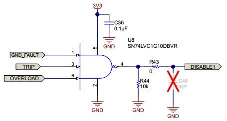
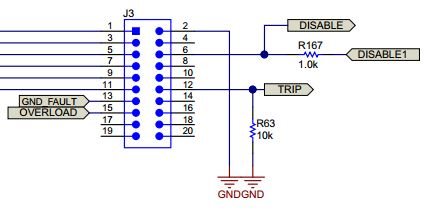
I am advancing with the programming of my inverter (TIDA-00366)! However, there is still a problem: In the PDFs of the reference design TIDA-00366 it is mentioned that one shall change the status of one GPIO pin from input to output for a short time to drag the potential of the DISABLE signal down to GND. Because at power-up of the board the DISABLE potential is high and blocks all PWM signals of the gate drivers.
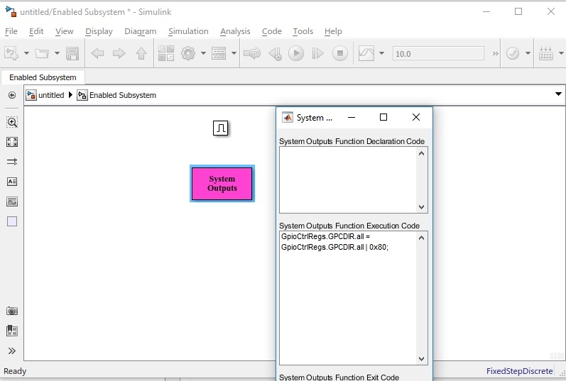
But my problem is that I cannot change the status of the GPIO pin during runtime in Simulink. If I have the same GPIO pin as input and output in my model, Simulink always throws an error when compiling the C code. Even when I use enabled subsystems to prevent the input and output block of the one GPIO to be active at the same time.
Do you know how I could solve the problem? I attached images of the schematics that may help you to understand my problem.
PS: I cannot set the GPIO status to output all the time because then the MCU would dictate the potential of the DISABLE signal. But the DISABLE signal should be set high by the logic gate during operation of the inverter (if an error occurs).
Best regards,
Armin


