Because of the holidays, TI E2E™ design support forum responses will be delayed from Dec. 25 through Jan. 2. Thank you for your patience.

This thread has been locked.

If you have a related question, please click the "Ask a related question" button in the top right corner. The newly created question will be automatically linked to this question.

TMS320F28379D: Signal Conditioning Circuit Recommendation

Part Number: TMS320F28379D
Other Parts Discussed in Thread: THS4551, REF3330

Hi,

Can you help with my customer's request below:

There is a requirement for simultaneous sampling of 4 currents (4 pole bridge. Can use 12-bit here).
Also I have General Purpose Analog Input that needs 16-bit resolution.

Based on these two requirements we have chosen 16-bit for all ADCs: A,B,C,D because of that one channel.

We have tight pcb constraints.
What would be minimum signal conditioning circuit to meet ADC requirements (like correct CM).

Can we configure DSP to run all ADC channels in 12-bit mode and switch to 16-bit and back on the fly for that single channel conversion?

Thanks,

Chuchen

  • Hi Chuchen,

    You can switch between resolutions.  Please see this thread and the additional linked threads inside:

    As far as signal conditioning circuitry, a single fully-differential op-amp will probably be the easiest and most space-efficient solution for 16-bit sampling. e.g. THS4531, but there are also topologies that use 2 single-ended op-amps to drive the differential signal.  

    Your best bet here is probably to create a new thread in the precision amplifiers forum to get help with designing a circuit and selecting a part for ADC signal conditioning.

  • Hi Devin,

    Can you share some insight on question below?

    Delfino’s ADC are in 16 bit mode, true differential. 7 channels total.  Although I need only one channel to be 16-bit, and so differential, while the rest 12-bit, single ended, 4 of these channels will be used for current sampling, so they come in pairs, simultaneous sampling.  I had to make all differential, because we do not know if we can have different resolution 12 bit for most, and 16 bit for one.  There is information online, but very confusing. It seems that we would have to sacrifice some performance of ADCs if I switch resolution on the fly. True or not?

    Below feedback is regarding analog signal conditioning, I'm looking into this separately but any recommendation is welcome:

    ---

    But board space is very critical in this design. I am using 201s for most comports. Having smaller footprint analog signal conditioning would help a lot.   

    I am using REF3330AIRSER fixed 3V reference, 0.15% initial tolerance, kind of noisy and temp.comp on the higher side, but I cannot find small part. Hope it works for me.  THS4551 op amp drivers for most of the channels with some filtering. +1.5 offset reference.  To use full ADC dynamic range, I have split power supply, +3V and -1.5V for op amp signal conditioning to get to true zero voltage.

    Thanks,

    Chuchen

  • Hi Chuchen,

    If you want to simultaneously sample, you can actually do this for 4 channels at once and there is no need for the channels to have matched numbers like on previous devices (e.g. you can use A1 and B3 and C2 and D1 to get 4 simultaneous samples).

    It's fine to mix resolutions, you just need to trigger the samples separately. So you might do something like:

    *All 4 ADCs start in 12-bit mode
    *ePWM triggers 4 simultaneous 12-bit conversions (say A0, B0, C2, D0)
    *ISR reads all 4 conversions, switches the resolution of ADC-A to 16-bit, and then SW triggers ADC A1
    *Another ISR reads the 16-bit result for A1 and switches the resolution of ADC-A back to 12-bit so that the next ePWM trigger can trigger all 4 ADCs in parallel in 12-bit mode

    Are you using a buffer to drive the VREFHI pins, or the REF3330 directly? I'm not sure you'll get good performance, especially in 16-bit mode, if you don't buffer the reference.
  • Hi Devin,

    Thanks for the quick reply.

    Reference is buffered with op amps.
    4 - op amps with 22uF at the outputs of each. Like in the reference design.
    There are 0.1 Ohm series resistor to fix response.
    Do we really need to use this large bank of 88uF?

    Thanks,
    Chuchen
  • Hi Chuchen,

    You definitely need the capacitance; a 16-bit LSB is only 3.0V/65536 = 46uV, so the reference voltage needs to be very stable and low noise.

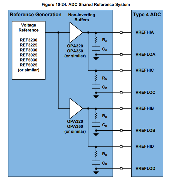
    You can, however, share 2 VREFHI channels between one op-amp output with minimal performance degradation.
  • Hi Devin,

    As mentioned previously, the customer is using 4 op-amps with 22uF at the outputs of each. They want to drop two 22uF caps out of 4, and use only total of 44uF because of PCB space constraints. How critical is this?
    They will drop the caps and adjust buffers to reflect lower capacitive load. There are only 7 ADC channels in their design. All are 12-bit.

    Thanks,
    Chuchen
  • Hi Chuchen,

    If they are only using 12-bit they can reduce the capacitance per-pin to 2.2uF, which probably allows a smaller package.

    If they are using 4 op-amps, they definitely need 4 capacitors.  Otherwise a pin won't have any capacitance (the reference pins are not connected internally).

    I'd still recommend one capacitor per-pin, but, as previously discussed, they should be able to use 2 op-amps instead of 4 (and use 4 capacitors). See this illustration in the TRM:

  • Hi Devin,

    Further feedback from customer:

    Please confirm that total capacitance can be 8.8uF for 12-bit converter.
    Separate caps preferred. 4 x 2.2uF, right?

    Is it 2.2uF per ADC reference pin? Pins are VREFHIA, VREFHIB, VREFHIC, and VREFHID.
    That makes it total of 8.8uF. That is 10 times less compare to 16-bit mode, right?

    I will use two op amps. One for VREFHIA and VREFHIC and one for VREFHIB and VREFHID. Like it is in your drawing.

    Thanks,
    Chuchen
  • Hi Chuchen,

    Yes, that understanding is correct. Note that with smaller capacitors the series snubbing resistors can be reduced or eliminated, depending on the driving op-amp's ability to drive a capacitive load.

    In addition, the capacitors should be placed as close as possible to the VREFHI and VREFLO pins.  This should be one of the highest layout constraints for the PCB design.  The distance from the op-amps to the VREFHI pins should also be kept reasonably short (to avoid picking up noise in the reference signal).