This thread has been locked.

If you have a related question, please click the "Ask a related question" button in the top right corner. The newly created question will be automatically linked to this question.

TMS320F28377D: Differential SAR Driver

Part Number: TMS320F28377D
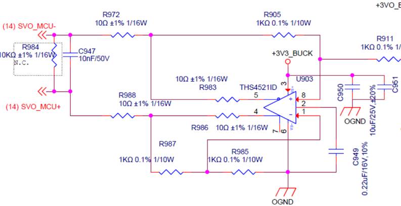
Other Parts Discussed in Thread: THS4521

Hi Team,

Mu customer is using 28377D SAR ADC, and trying to use differential op-amp THS4521 as a  input driver.

They are using 16b mode.  I am not sure sampling rate, but let's assume 1MSPS.

28377D datasheet is too complicated to read for me, may I ask one simple question.

For driver output R and C, can I use something like below?

If not, what is appropriate values? 

By the way, if 28377D SAR internal model is available, I would like to have it so I can play with it, thanks a lot.

Andrew

  • Hi Andrew,

    There is actually an input model of the ADC available in the DS:

    www.ti.com/.../specifications

    If you want to play around with this model in TINA (or some other circuit simulator) it should be easy enough to setup. Basically you can build the input circuit plus the ADC model and then simulate the following:
    *Initial condition: ADC Ch is at 0V
    *Initial condition: ADC Cp and external circuit C947 are pre-charged to 2.5V (or whatever you want to use as the max ADC input voltage).
    *Op-amp input = 2.5V DC input
    *-->(1) How long does it take for Ch to charge to within 0.25 LSBs of 2.5V? (this determines the minimum S+H)
    *-->(2) After the conversion, how long does it take for C947 to recover to within 0.25LSBs of 2.5V (this determines the maximum sample rate on that pin)

    Some notes:
    *Start with an ideal voltage source instead of the op-amp
    *When you add the op-amp effect, use an ideal op-amp and then set the BW and Slew rate of the THS4521 in that model. Using the THS4521 model directly can be tricky because it includes additional errors (e.g. Vos) which causes the circuit to no longer settle to 2.5V exactly.
    *Usually only simulation (1) or (2) will be done, not both.
    -->Typically the source capacitance, Cs (C947), is set to 10x to 30x Ch to achieve maximum sample rate. This would be much less than 10nF. In this case, only simulation (1) would be done to determine the required S+H duration
    -->If sample rate on the pin is less important (e.g. maybe a 10kHz ePWM is driving the conversions), then Cs is selected to be at least (2^(N+1))*Ch. This would probably be more than 10nF, especially in 16-bit mode. In this case, minimum S+H can be used (because all the charge comes from Cs) but simulation (2) must be done to select a sample rate that is not too fast, otherwise charge will slowly bleeds off of Cs with each successive conversion.