This thread has been locked.

If you have a related question, please click the "Ask a related question" button in the top right corner. The newly created question will be automatically linked to this question.

TMS320F28054M: 28054M MCU locked at debug

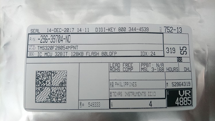
Part Number: TMS320F28054M
Other Parts Discussed in Thread: UNIFLASH, MOTORWARE

I want to program 28054M mcu with XDS100 emulator at my own board. I compile lab02a of Instaspin and can easily download and run it with 28054F device. Nevertheless, when I try to use 28054M at the same hardwareI have several problems.

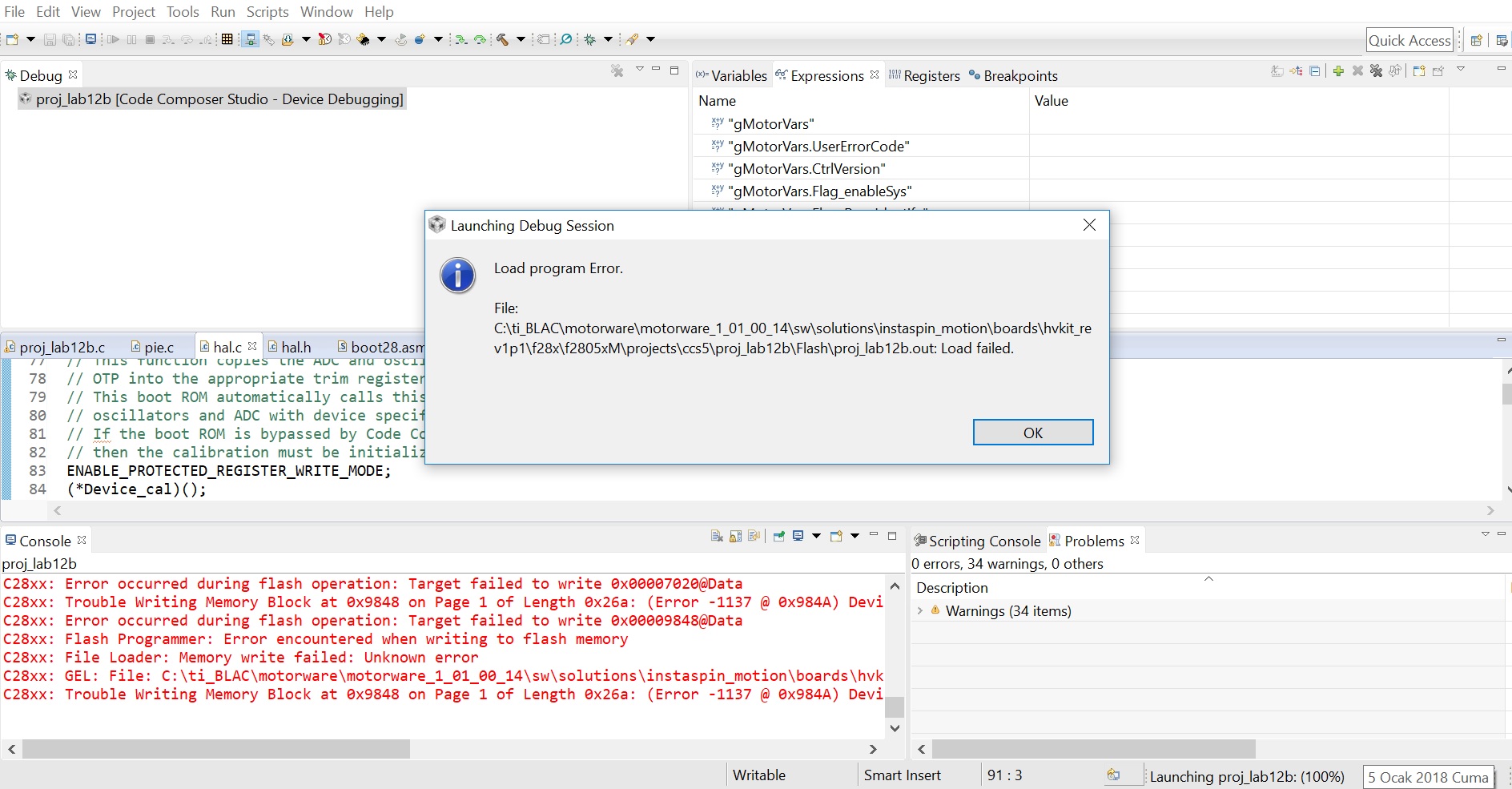
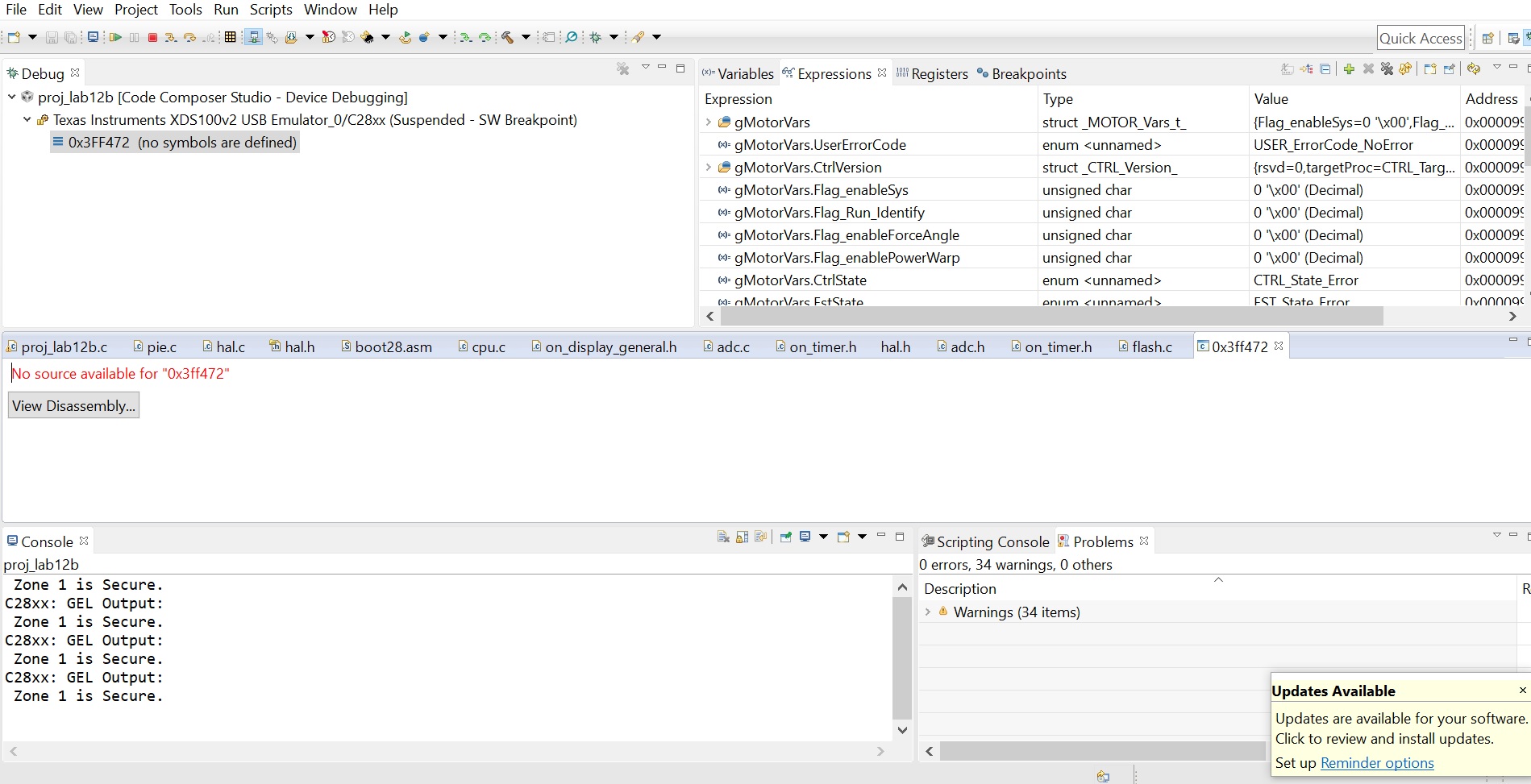
In debug mode, we can download the code to flash to 28054M. When we run it, it works first then the mcu is locked. You can see the debug window below. Then we cannot reach the mcu with any program like Uniflash etc. What could be the reason?

  • Hi,

    Have you locked the part with the CSM?

    sal

  • Hi,

    Not very clear on the issue you are facing. What is the error message you are getting? Can you attach the full snapshot of CCS window including the error message.

    Vivek Singh

  • You can see the message below:

    When I try to connect again I see this message

    Also in Uniflash I see foloowing message when I try to read its flash

  • Hi,

    Can you send screen shots of the top view of the two devices you are using, please? We want to see what is printed on the parts.

    sal

  • Following codes are written on the parts:

    TMS320

    F28054MPNT

    C   A-62ANVEW

                G4

    Below you can find the view of package:

  • We need screenshot of other device as well. On these devices, TI locks Zone1 and L0 RAM so user need not to use L0 in their application. I hope that is taken care in your application.

    Also have you tried this on just one board with M part of multiple parts?

    Vivek Singh
  • You can find screenshot for 28054F below. There is no problem with that mcu:

    I just try to download original code of motorware. There is no additional code. I do not understand why such a condition occurs. I observe that this error happens in some of my trials. Maybe I try six or seven times there is no problem. But for the next trial this error occurs.

  • I have written screenshots of the two devices in the messages above. I could not solve the problem yet.

    In your demoboard schematics (f2806x iso-controlcard and F2805X_ISOcCARD) there is a difference. In 2805x schemtaic you have an additional 2.2k pull up at JTAG_TCK. Can it be an issue to cause such a problem?

    Moreover, I have a double layer pcb. I do not think that it can cause such a problem but I see in you demo designs that you recommend 4layer or more at pcb while using C2000 series. Do you advise me to use a 4 layer pcb design?

    I have also taken screenshots of emulator screen just before the problem and just after it. First is just before the problem, every variable has a ridicolous value with a BAD sign. 

    Then it just stops at some program memory point 3FF472. I think this is a point in ROM

  • I am asking our board designer to look into your recent queries.

    Vivek Singh
  • ok thanks I am waiting for your comments
  • Motor_Enthusiast,

    There is an internal pull-up on TCK, an external pull-up resistor is not required.

    I expect that a 2 layer board would likely not be the cause, a 2 layer board will be more susceptible to noise because its lacking power or ground planes, but this shouldnt affect your ability to connect to the device in relatively "clean" noise environment. 

    The 0x0BAD is just a general lack of communication between CCS and the device.

    My theory is that you interrupted the device while programming or erasing the flash causing the password locations to be corrupted. This means you will be locked out of the device. Please check the "CSM control registers", this will indicate if the device is locked. The location and a description of the bits can be found in the TRM, 

    Regards,
    Cody 

  • I realized one thing in Instaspin motorware projects. In hal.c file there is a HAL_cal function that is used to calibrate adc and oscillator calibration. For 28069M device, it is like this:

    void HAL_cal(HAL_Handle handle)

    {

     HAL_Obj *obj = (HAL_Obj *)handle;

     // enable the ADC clock

     CLK_enableAdcClock(obj->clkHandle);

     // Run the Device_cal() function

     // This function copies the ADC and oscillator calibration values from TI reserved

     // OTP into the appropriate trim registers

     // This boot ROM automatically calls this function to calibrate the interal

     // oscillators and ADC with device specific calibration data.

     // If the boot ROM is bypassed by Code Composer Studio during the development process,

     // then the calibration must be initialized by the application

     ENABLE_PROTECTED_REGISTER_WRITE_MODE;

     (*Device_cal)();

     DISABLE_PROTECTED_REGISTER_WRITE_MODE;

     // run offsets calibration in user's memory

     HAL_AdcOffsetSelfCal(handle);

     // run oscillator compensation

     HAL_OscTempComp(handle);

     // disable the ADC clock

     CLK_disableAdcClock(obj->clkHandle);

     return;

    } // end of HAL_cal() function

    But for 28054M device HAL_OscTempComp(handle);     line is removed via // comment. ADC conversion result was wrong for 28054M device so I have just compared ADC register settings for 28054M and 28069M. Then I realize that for 28054M device ADCCTL2 register ADCNONOVERLAP bit is 0 so overlap of sample and conversion is allowed. On the other hand, this bit was 1 for 28069M device.

    To set this bit I removed the comment for HAL_OscTempComp(handle); but at that case mcu is locked as I describe you. Whenever I comment HAL_OscTempComp(handle);  function mcu works without any lock but ADC conversion results are wrong.

    You can find the HAL_OscTempComp(handle);  function below:

    void HAL_OscTempComp(HAL_Handle handle)

    {

     HAL_Obj *obj = (HAL_Obj *)handle;

     uint16_t Temperature;

     // disable the ADCs

     ADC_disable(obj->adcHandle);

     // power up the bandgap circuit

     ADC_enableBandGap(obj->adcHandle);

     // set the ADC voltage reference source to internal

     ADC_setVoltRefSrc(obj->adcHandle,ADC_VoltageRefSrc_Int);

     // enable the ADC reference buffers

     ADC_enableRefBuffers(obj->adcHandle);

     // Set main clock scaling factor (max45MHz clock for the ADC module)

     ADC_setDivideSelect(obj->adcHandle,ADC_DivideSelect_ClkIn_by_2);

     // power up the ADCs

     ADC_powerUp(obj->adcHandle);

     // enable the ADCs

     ADC_enable(obj->adcHandle);

     // enable non-overlap mode

     ADC_enableNoOverlapMode(obj->adcHandle);

     // connect channel A5 internally to the temperature sensor

     ADC_setTempSensorSrc(obj->adcHandle, ADC_TempSensorSrc_Int);

     // set SOC0 channel select to ADCINA5

     ADC_setSocChanNumber(obj->adcHandle, ADC_SocNumber_0, ADC_SocChanNumber_A5);

     // set SOC0 acquisition period to 26 ADCCLK

     ADC_setSocSampleDelay(obj->adcHandle, ADC_SocNumber_0, ADC_SocSampleDelay_64_cycles);

     // connect ADCINT1 to EOC0

     ADC_setIntSrc(obj->adcHandle, ADC_IntNumber_1, ADC_IntSrc_EOC0);

     // clear ADCINT1 flag

     ADC_clearIntFlag(obj->adcHandle, ADC_IntNumber_1);

     // enable ADCINT1

     ADC_enableInt(obj->adcHandle, ADC_IntNumber_1);

     // force start of conversion on SOC0

     ADC_setSocFrc(obj->adcHandle, ADC_SocFrc_0);

     // wait for end of conversion

     while (ADC_getIntFlag(obj->adcHandle, ADC_IntNumber_1) == 0){}

     // clear ADCINT1 flag

     ADC_clearIntFlag(obj->adcHandle, ADC_IntNumber_1);

     Temperature = ADC_readResult(obj->adcHandle, ADC_ResultNumber_0);

     HAL_osc1Comp(handle, Temperature);

     HAL_osc2Comp(handle, Temperature);

     return;

    } // end of HAL_OscTempComp() function

    Then I have several questions:

    1) What is the difference between ADCNONOVERLAP value 0 and 1 in application? Can a zero value at that bit result a wrong ADC conversion? There is no detailed explanation for that bit in TRM.

    2) Why is the function HAL_OscTempComp() commented for 28054 device while it is active for 28069?

    3)Why does activating HAL_OscTempComp() function lead to a lock in mcu for 28054M device?

  • M.E.,

    It looks like the HAL software was not properly ported to F2805x.  The OTP functions used by oscNComp() are located in different locations between F2806x and F2805x so that would explain your execution fault if the addresses were not updated in software.  The correct implementation would have been to update the OTP function addresses and include HAL_OscTempComp().  With just Device_cal(), the oscillators will be trimmed for 30C operation.

    Both F2806x and F2805x have an ADC Advisory for Initial Conversion error that can be reduced by setting the ADCNONOVERLAP bit.  The difference in ADCNONOVERLAP behavior is subtle.

    For the figure below with ADC overlap allowed (ADCNONOVERLAP=0), the ADC can begin sampling the SOC1 channel while the SOC0 conversion is still being processed:

    When ADC overlap is not allowed (ADCNONOVERLAP=1), the ADC will not begin sampling the SOC1 channel until the SOC0 conversion is complete:

    Please also be aware that the F2805x datasheet includes recommended ACQPS settings that vary depending on the ADCNONOVERLAP setting:

    -Tommy

  • Thank you for the reply, the linker command file that comes with motorware is nearly the same with the one that comes with CCS studio setup. The only difference I see is that in motorware C to F sections of flash are unified. You can find the map file below, is there any problem with that:

    MEMORY
    {
    PAGE 0: /* Program Memory */
    /* Memory (RAM/FLASH/OTP) blocks can be moved to PAGE1 for data allocation */
    RAML1L2 : origin = 0x008800, length = 0x000800 /* on-chip RAM block L1 */
    FLASHJ : origin = 0x3E8000, length = 0x001000 /* on-chip FLASH */
    FLASHI : origin = 0x3E9000, length = 0x001000 /* on-chip FLASH */
    FLASHH : origin = 0x3EA000, length = 0x002000 /* on-chip FLASH */
    FLASHG : origin = 0x3EC000, length = 0x002000 /* on-chip FLASH */
    /* FLASHF : origin = 0x3EE000, length = 0x002000 /* on-chip FLASH */
    /* FLASHE : origin = 0x3F0000, length = 0x002000 /* on-chip FLASH */
    /* FLASHD : origin = 0x3F2000, length = 0x002000 /* on-chip FLASH */
    FLASHC_F : origin = 0x3EE000, length = 0x008000 /* on-chip FLASH */
    FLASHA : origin = 0x3F7000, length = 0x000FFE /* on-chip FLASH */
    BEGIN : origin = 0x3F7FFE, length = 0x000002 /* Part of FLASHA. Used for "boot to Flash" bootloader mode. */

    Z1_SCC_ROM : origin = 0x3F8000, length = 0x000400 /* Zone 1 Safe-Copy Code Secure ROM */
    Z2_SCC_ROM : origin = 0x3F8400, length = 0x000400 /* Zone 2 Safe-Copy Code Secure ROM */
    Z1_SECURE_ROM : origin = 0x3F8808, length = 0x0044F8 /* Z1 Secure ROM */

    IQTABLES : origin = 0x3FDB52, length = 0x000b50 /* IQ Math Tables in Boot ROM */
    IQTABLES2 : origin = 0x3FE6A2, length = 0x00008C /* IQ Math Tables in Boot ROM */
    IQTABLES3 : origin = 0x3FE72E, length = 0x0000AA /* IQ Math Tables in Boot ROM */


    DCSM_OTP_Z2_P0 : origin = 0x3D7800, length = 0x000004 /* Part of Z1 OTP. LinkPointer/JTAG lock/ Boot Mode */
    DCSM_OTP_Z1_P0 : origin = 0x3D7A00, length = 0x000006 /* Part of Z2 OTP. LinkPointer/JTAG lock */

    /* DCSM Z1 Zone Select Contents and Reserved Locations (!!Movable!!) */
    /* Z1_DCSM_RSVD must be programmed to all 0x0000 and must immediately follow Z1 Zone Select block */
    DCSM_ZSEL_Z1_P0 : origin = 0x3D7A10, length = 0x000010 /* Part of Z1 OTP. Z1 password locations / Flash and RAM partitioning */
    Z1_DCSM_RSVD : origin = 0x3D7A20, length = 0x0001E0 /* Part of Z1 OTP. Program with all 0x0000 when Z1 DCSM is in use. */

    /* DCSM Z1 Zone Select Contents and Reserved Locations (!!Movable!!) */
    /* Z2_DCSM_RSVD must be programmed to all 0x0000 and must immediately follow Z2 Zone Select block */
    DCSM_ZSEL_Z2_P0 : origin = 0x3D7810, length = 0x000010 /* Part of Z2 OTP. Z2 password locations / Flash and RAM partitioning */
    Z2_DCSM_RSVD : origin = 0x3D7820, length = 0x0001E0 /* Program with all 0x0000 when Z2 DCSM is in use. */

    ROM : origin = 0x3FF27C, length = 0x000D44 /* Boot ROM */
    RESET : origin = 0x3FFFC0, length = 0x000002 /* part of boot ROM */
    VECTORS : origin = 0x3FFFC2, length = 0x00003E /* part of boot ROM */

    PAGE 1 : /* Data Memory */
    /* Memory (RAM/FLASH/OTP) blocks can be moved to PAGE0 for program allocation */
    /* Registers remain on PAGE1 */
    BOOT_RSVD : origin = 0x000000, length = 0x000050 /* Part of M0, BOOT rom will use this for stack */
    RAMM0 : origin = 0x000050, length = 0x0003B0 /* on-chip RAM block M0 */
    RAMM1 : origin = 0x000400, length = 0x000400 /* on-chip RAM block M1 */
    RAML3 : origin = 0x009000, length = 0x001000 /* on-chip RAM block L3 */
    FLASHB : origin = 0x3F6000, length = 0x001000 /* on-chip FLASH */

    }

    /* Allocate sections to memory blocks.
    Note:
    codestart user defined section in DSP28_CodeStartBranch.asm used to redirect code
    execution when booting to flash
    ramfuncs user defined section to store functions that will be copied from Flash into RAM
    */

    SECTIONS
    {

    /* Allocate program areas: */
    .cinit : > FLASHC_F PAGE = 0
    .pinit : > FLASHC_F, PAGE = 0
    .text : > FLASHC_F PAGE = 0
    codestart : > BEGIN PAGE = 0

    ramfuncs : LOAD = FLASHA,
    RUN = RAML1L2,
    LOAD_START(_RamfuncsLoadStart),
    LOAD_END(_RamfuncsLoadEnd),
    RUN_START(_RamfuncsRunStart),
    PAGE = 0

    dcsm_otp_z1 : > DCSM_OTP_Z1_P0 PAGE = 0
    dcsm_otp_z2 : > DCSM_OTP_Z2_P0 PAGE = 0

    dcsm_zsel_z1 : > DCSM_ZSEL_Z1_P0 PAGE = 0
    dcsm_rsvd_z1 : > Z1_DCSM_RSVD PAGE = 0
    dcsm_zsel_z2 : > DCSM_ZSEL_Z2_P0 PAGE = 0
    dcsm_rsvd_z2 : > Z2_DCSM_RSVD PAGE = 0

    /* Allocate uninitalized data sections: */
    .stack : > RAMM0 PAGE = 1
    .ebss : > RAML3 PAGE = 1
    .esysmem : > RAML3 PAGE = 1

    /* Initalized sections go in Flash */
    /* For SDFlash to program these, they must be allocated to page 0 */
    .econst : > FLASHC_F PAGE = 0
    .switch : > FLASHC_F PAGE = 0

    /* Allocate IQ math areas: */
    IQmath : > FLASHC_F PAGE = 0 /* Math Code */
    IQmathTables : > IQTABLES, PAGE = 0, TYPE = NOLOAD

  • That should be fine as far as I know.
  • We have solved the ADC problem. I think for 28054 device there is a problem at ADC input which are connected to PGA. Even if you do not use PGA functionality there is a gain at that pins so you cannot set it to 1. When I moved the readings to pins that are not connected to PGA, ADC readings become correct. There are also similar discussions at E2E forum about that.

    On the other hand, mcu lock problem still continues. I have realized that it results from

     HAL_osc1Comp(handle, Temperature);

     HAL_osc2Comp(handle, Temperature);

    Functions in HAL_OscTempComp

    You say that OTP function addresses of 2806x and 2805x are different. Is it possible to have a problem of addresses defined in 2805x header file? Because I see that those addresses are defined as completely the same for 2806x and 2805x. You can find the hal.h file at the attachment for 2805x. Is there any problem with the addresses defined at that file?

    0028.hal.h

  • It seems like you are using a previous motorware version, maybe v14 or earlier. The defines at temperature sensor registers are not correct in hal.h in these previous versions, so we commented the oscillator compensation function, HAL_OscTempComp(handle) in hal.c. These incorrect defines will cause the PC go into error address if you call the HAL_OscTempComp().

    We have fixed this issue from motorware V15, the latest version is V18 which also fixed this issue, you may use the new hal.h in your project or use the latest motorware.
  • Yes you are right I was using motorware 14. Then I have just moved the code to motorware 18. Now there is no problem of lock.

    But I have one more problem, I just download code via XDS100 emulator in debug mode using Code Composer Studio. Then I remove the emulator and everything seems like fine there is the code inside mcu. But when I cycle the power of the board. Board does not work again.

    I can read the memory using Uniflash, it seems that there is some code inside. But it does not work, there is not even a response in blinking led etc. so it means main_isr does not work.

    Similarly when I try to download the code via Uniflash, it does not work again. Only working option is debug operation via Code Composer Studio.

    What should be the reason?
  • Hi,

    You may have old code programmed in flash. You can use CCS to flash program your motorware code using a flash linker command file. Then, if you boot to flash, the application should start running as long as you have included the CodeStartBranch.asm file into your flash project.

    sal
  • Ok but, I am already using linker command file F28054M.cmd that is given in motorware18. CodeStartBranch.asm is also included in the project.
  • Hi,

    Can you ensure that your device is booting to flash? If your flash image is up to date, and your device is set to branch to flash on reset in standalone, then everything should work fine. Please ensure that your the LB instruction places at BEGIN (0x3F7FFE) is branching to your updated flash image. It should be branching to c_init.

    To ensure this, you can connect the debugger and move the PC to 0x3F7FFE and then run. Set a breakpoint at your main, and the PC should eventually halt at that address. This would let you know that you have your proper flash image programmed. And the ROM could successfully branch to it and begin executing your application.

    Hope this helps.
    sal
  • I see that LB instruction places at BEGIN(0x37FFE)

    In disassembly window I see that 007F3CF7 is written on program address 0x3F7FFE.

    When I cycle the power and read the same address via Uniflash I see that again 007F3CF7 is written. But somehow the program does not work after power reset.

    I also bought your 28054MISO control board and tried it with your High Voltage kit. But I could not try it with a poweron reset because it gets in reset state after power on (I think this results from the on-board XDS100 emulator, ı cannot remove the emulator on the demo board)

    How should I continue?
  • Hi,

    With the emulator connected, set the device to boot to Flash, even in emulation mode. Chapter 2 of the TRM will have this information. Then you can debug your system.

    So, set the device to boot to flash (emu boot) and set a breakpoint at BEGIN, then you can begin to debug your code.

    Additionally, you can connect to the device, move the PC to BEGIN and run. You can start debugging your system this way as well.

    Hope this helps.
    sal