This thread has been locked.

If you have a related question, please click the "Ask a related question" button in the top right corner. The newly created question will be automatically linked to this question.

F28M35H52C: a little confuse about C28 GPIO port E clock

Part Number: F28M35H52C

Hi, the clock source of GPIO PORT E seems different from PORT A,B and C. In page 376 of spruh22h, it is described that 

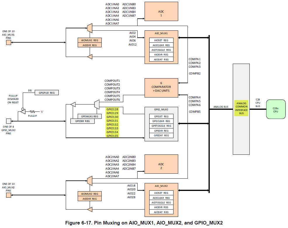
By default, GPIO Port A, B, and C are synchronized to SYSCLKOUT only, and GPIO Port E is synchronized to the analog subsystem clock.

but in page 409, when given the description of GPIOEQSEL1 register, however, it is described that :

00 Synchronize to SYSCLKOUT only. Valid for both peripheral and GPIO pins.
01 Qualification using 3 samples. Valid for pins configured as GPIO or a peripheral function. The time between samples is specified in the GPECTRL register.

So, which one should I refer to about Port E clock? and if GPIO Port E is synchronized to the analog subsystem clock,  dose it mean that the clock of GPIO port E should not exceed the maximum frequency of 37.5 MHz? Thanks!

  • Guanglei,

    Yes, GPIO Port E will be synchronized to the analog subsystem clock. If you look at the input qualification section 4.2.5  of the same document each of the options are described in more detail.

    If you are using input qualification: Then signals faster than the analog subsystems clock will be missed.

    Please also look at section 5.9.6.2 "GPIO - Input Timing" from the Datasheet this describes some of the speed limitations of the different GPIO Input timings.

    Regards,
    Cody

  • Cody,

    Thanks for your reply. Actually, I'm much more interested in the output characteristics of GPIO port E. I've checked in the datasheet 5.9.6.1. It's given that  the Toggling maxium frequency  is 25MHz. Then i tested as follows:

    while(1)

    {

     GpioG2DataRegs.GPETOGGLE.bit.GPIO129 = 1;

    asm("rpt #03 || nop");

    }

    (C28 SYSCLOCK = 75MHz, CCLKCTL = 0x4)

    observed by the oscilloscope, GPIO129 output  is a square wave of 270KHz. Sounds wierd! Then i checked the disassembly code. The inner loop code is listed as follows:

    MOVW DP, #0x1bf

    OR      @0x6, #0x0002 

    RPT #3

    || NOP

    With the help of CCS clock profile, "OR      @0x6, #0x0002 " takes almost  64 C28 SYSCLOCKs. I can't figure out what the problem is. Would you please help me out?

    Regards,

    Guanglei

  • Guanglei,

    The registers for the Port E GPIO pins are accessed through the Analog Common Interface Bus (ACIB).  You can see the Analog Subsystem section in the TRM for timing diagrams of read and write operations across the ACIB.

    -Tommy

  • Thanks, Tommy. The figure is clear.

    Regards,

    Guanglei