Part Number: TMS320F28069F
Other Parts Discussed in Thread: CONTROLSUITE
Hi !
I want to know is there any difference beetween TMS320F28069FPZT and TMS320F28069UPZT ? Because I'm cannot running TMS320F28069FPZT based board...
Thanks !
This thread has been locked.
If you have a related question, please click the "Ask a related question" button in the top right corner. The newly created question will be automatically linked to this question.
Part Number: TMS320F28069F
Other Parts Discussed in Thread: CONTROLSUITE
Hi !
I want to know is there any difference beetween TMS320F28069FPZT and TMS320F28069UPZT ? Because I'm cannot running TMS320F28069FPZT based board...
Thanks !
Hi,
eeddii iiiiii said:I want to know is there any difference beetween TMS320F28069FPZT and TMS320F28069UPZT ? Because I'm cannot running TMS320F28069FPZT based board...
F28069F part is a FOC part for motor control. F28069U is the generic F28069 with USB functionality.
Regards,
Gautam
eeddii iiiiii said:Can I use 28069FPZT instead of 28069UPZT ?
Yes, you can. F28069U is a subset of F28069F.
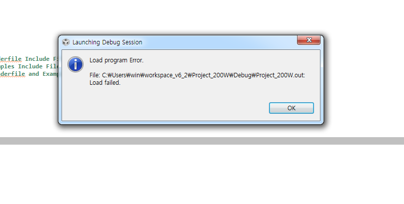
eeddii iiiiii said:I cannot upload the devce(28069FPZT) . There is below me
Check you target configuration. Also, please Rebuild your code (Using 'Rebuild' option)
Regards,
Gautam
Ok,
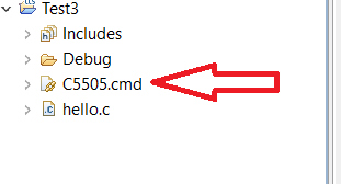
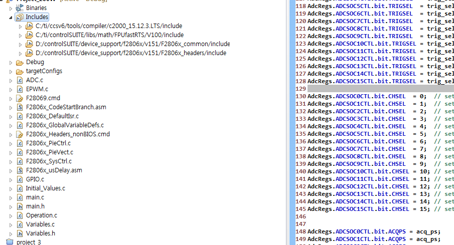
Why there are two command files in this project folder?
Would you click on both of them and take a snapshot of them and send back to me?
Yes ...There's F28069.cmd :
MEMORY
{
PAGE 0 : /* Program Memory */
/* Memory (RAM/FLASH/OTP) blocks can be moved to PAGE1 for data allocation */
RAML0 : origin = 0x008000, length = 0x002000 /* on-chip RAM block L0 */
// RAML1 : origin = 0x008800, length = 0x000400 /* on-chip RAM block L1 */
OTP : origin = 0x3D7800, length = 0x000400 /* on-chip OTP */
FLASHH : origin = 0x3D8000, length = 0x004000 /* on-chip FLASH */
FLASHG : origin = 0x3DC000, length = 0x004000 /* on-chip FLASH */
FLASHFE : origin = 0x3E0000, length = 0x008000 /* on-chip FLASH */
// FLASHE : origin = 0x3E4000, length = 0x004000 /* on-chip FLASH */
FLASHA : origin = 0x3F4000, length = 0x003F80 /* on-chip FLASH */
CSM_RSVD : origin = 0x3F7F80, length = 0x000076 /* Part of FLASHA. Program with all 0x0000 when CSM is in use. */
BEGIN : origin = 0x3F7FF6, length = 0x000002 /* Part of FLASHA. Used for "boot to Flash" bootloader mode. */
CSM_PWL_P0 : origin = 0x3F7FF8, length = 0x000008 /* Part of FLASHA. CSM password locations in FLASHA */
FPUTABLES : origin = 0x3FD860, length = 0x0006A0 /* FPU Tables in Boot ROM */
IQTABLES : origin = 0x3FDF00, length = 0x000B50 /* IQ Math Tables in Boot ROM */
IQTABLES2 : origin = 0x3FEA50, length = 0x00008C /* IQ Math Tables in Boot ROM */
IQTABLES3 : origin = 0x3FEADC, length = 0x0000AA /* IQ Math Tables in Boot ROM */
ROM : origin = 0x3FF3B0, length = 0x000C10 /* Boot ROM */
RESET : origin = 0x3FFFC0, length = 0x000002 /* part of boot ROM */
VECTORS : origin = 0x3FFFC2, length = 0x00003E /* part of boot ROM */
PAGE 1 : /* Data Memory */
/* Memory (RAM/FLASH/OTP) blocks can be moved to PAGE0 for program allocation */
/* Registers remain on PAGE1 */
BOOT_RSVD : origin = 0x000000, length = 0x000050 /* Part of M0, BOOT rom will use this for stack */
RAMM0 : origin = 0x000050, length = 0x0003B0 /* on-chip RAM block M0 */
RAMM1 : origin = 0x000400, length = 0x000400 /* on-chip RAM block M1 */
RAML2 : origin = 0x00A000, length = 0x002000 /* on-chip RAM block L2 */
// RAML3 : origin = 0x009000, length = 0x001000 /* on-chip RAM block L3 */
// RAML4 : origin = 0x00A000, length = 0x002000 /* on-chip RAM block L4 */
RAML5 : origin = 0x00C000, length = 0x002000 /* on-chip RAM block L5 */
RAML6 : origin = 0x00E000, length = 0x002000 /* on-chip RAM block L6 */
RAML7 : origin = 0x010000, length = 0x002000 /* on-chip RAM block L7 */
RAML8 : origin = 0x012000, length = 0x002000 /* on-chip RAM block L8 */
USB_RAM : origin = 0x040000, length = 0x000800 /* USB RAM */
FLASHD : origin = 0x3E8000, length = 0x004000 /* on-chip FLASH */
FLASHC : origin = 0x3EC000, length = 0x004000 /* on-chip FLASH */
FLASHB : origin = 0x3F0000, length = 0x004000 /* on-chip FLASH */
}
/* Allocate sections to memory blocks.
Note:
codestart user defined section in DSP28_CodeStartBranch.asm used to redirect code
execution when booting to flash
ramfuncs user defined section to store functions that will be copied from Flash into RAM
*/
SECTIONS
{
/* Allocate program areas: */
.cinit : > FLASHFE, PAGE = 0
.pinit : > FLASHFE, PAGE = 0
.text : > FLASHFE, PAGE = 0
codestart : > BEGIN, PAGE = 0
ramfuncs : LOAD = FLASHH,
RUN = RAML0,
LOAD_START(_RamfuncsLoadStart),
LOAD_END(_RamfuncsLoadEnd),
RUN_START(_RamfuncsRunStart),
LOAD_SIZE(_RamfuncsLoadSize),
PAGE = 0
csmpasswds : > CSM_PWL_P0, PAGE = 0
csm_rsvd : > CSM_RSVD, PAGE = 0
/* Allocate uninitalized data sections: */
.stack : > RAMM0, PAGE = 1
.ebss : > RAML2, PAGE = 1
.esysmem : > RAML2, PAGE = 1
/* Initalized sections to go in Flash */
/* For SDFlash to program these, they must be allocated to page 0 */
.econst : > FLASHA, PAGE = 0
.switch : > FLASHFE, PAGE = 0
/* Allocate IQ math areas: */
IQmath : > FLASHFE, PAGE = 0 /* Math Code */
IQmathTables : > IQTABLES, PAGE = 0, TYPE = NOLOAD
/* Allocate FPU math areas: */
FPUmathTables : > FPUTABLES, PAGE = 0, TYPE = NOLOAD
DMARAML5 : > RAML5, PAGE = 1
DMARAML6 : > RAML6, PAGE = 1
DMARAML7 : > RAML7, PAGE = 1
DMARAML8 : > RAML8, PAGE = 1
/* Uncomment the section below if calling the IQNexp() or IQexp()
functions from the IQMath.lib library in order to utilize the
relevant IQ Math table in Boot ROM (This saves space and Boot ROM
is 1 wait-state). If this section is not uncommented, IQmathTables2
will be loaded into other memory (SARAM, Flash, etc.) and will take
up space, but 0 wait-state is possible.
*/
/*
IQmathTables2 : > IQTABLES2, PAGE = 0, TYPE = NOLOAD
{
IQmath.lib<IQNexpTable.obj> (IQmathTablesRam)
}
*/
/* Uncomment the section below if calling the IQNasin() or IQasin()
functions from the IQMath.lib library in order to utilize the
relevant IQ Math table in Boot ROM (This saves space and Boot ROM
is 1 wait-state). If this section is not uncommented, IQmathTables2
will be loaded into other memory (SARAM, Flash, etc.) and will take
up space, but 0 wait-state is possible.
*/
/*
IQmathTables3 : > IQTABLES3, PAGE = 0, TYPE = NOLOAD
{
IQmath.lib<IQNasinTable.obj> (IQmathTablesRam)
}
*/
/* .reset is a standard section used by the compiler. It contains the */
/* the address of the start of _c_int00 for C Code. /*
/* When using the boot ROM this section and the CPU vector */
/* table is not needed. Thus the default type is set here to */
/* DSECT */
.reset : > RESET, PAGE = 0, TYPE = DSECT
vectors : > VECTORS, PAGE = 0, TYPE = DSECT
}
/*
//===========================================================================
// End of file.
//===========================================================================
*/
And also F2806x_Headers_nonBIOS.cmd :
/*
//###########################################################################
//
// FILE: F2806x_Headers_nonBIOS.cmd
//
// TITLE: F2806x Peripheral registers linker command file
//
// DESCRIPTION:
//
// This file is for use in Non-BIOS applications.
//
// Linker command file to place the peripheral structures
// used within the F2806x headerfiles into the correct memory
// mapped locations.
//
// This version of the file includes the PieVectorTable structure.
// For BIOS applications, please use the F2806x_Headers_BIOS.cmd file
// which does not include the PieVectorTable structure.
//
//###########################################################################
// $TI Release: F2806x C/C++ Header Files and Peripheral Examples V151 $
// $Release Date: February 2, 2016 $
// $Copyright: Copyright (C) 2011-2016 Texas Instruments Incorporated -
// http://www.ti.com/ ALL RIGHTS RESERVED $
//###########################################################################
*/
MEMORY
{
PAGE 0: /* Program Memory */
PAGE 1: /* Data Memory */
DEV_EMU : origin = 0x000880, length = 0x000105 /* Device Emulation Registers */
SYS_PWR_CTL : origin = 0x000985, length = 0x000003 /* System Power Control Registers */
FLASH_REGS : origin = 0x000A80, length = 0x000060 /* Flash Registers */
CSM : origin = 0x000AE0, length = 0x000020 /* Code Security Module Registers */
ADC_RESULT : origin = 0x000B00, length = 0x000020 /* ADC Results Register Mirror */
CPU_TIMER0 : origin = 0x000C00, length = 0x000008 /* CPU Timer0 Registers */
CPU_TIMER1 : origin = 0x000C08, length = 0x000008 /* CPU Timer1 Registers */
CPU_TIMER2 : origin = 0x000C10, length = 0x000008 /* CPU Timer2 Registers */
PIE_CTRL : origin = 0x000CE0, length = 0x000020 /* PIE Control Registers */
PIE_VECT : origin = 0x000D00, length = 0x000100 /* PIE Vector Table */
DMA : origin = 0x001000, length = 0x000200 /* DMA Registers */
CLA1 : origin = 0x001400, length = 0x000080 /* CLA Registers */
USB0 : origin = 0x004000, length = 0x001000 /* USB0 Registers */
McBSPA : origin = 0x005000, length = 0x000040 /* McBSP-A Registers */
ECANA : origin = 0x006000, length = 0x000040 /* eCAN-A Control and Status Registers */
ECANA_LAM : origin = 0x006040, length = 0x000040 /* eCAN-A Local Acceptance Masks */
ECANA_MOTS : origin = 0x006080, length = 0x000040 /* eCAN-A Message Object Time Stamps */
ECANA_MOTO : origin = 0x0060C0, length = 0x000040 /* eCAN-A Object Time-Out Registers */
ECANA_MBOX : origin = 0x006100, length = 0x000100 /* eCAN-A Milboxes */
COMP1 : origin = 0x006400, length = 0x000020 /* Comparator + DAC 1 Registers */
COMP2 : origin = 0x006420, length = 0x000020 /* Comparator + DAC 2 Registers */
COMP3 : origin = 0x006440, length = 0x000020 /* Comparator + DAC 3 Registers */
EPWM1 : origin = 0x006800, length = 0x000040 /* Enhanced PWM 1 Registers */
EPWM2 : origin = 0x006840, length = 0x000040 /* Enhanced PWM 2 Registers */
EPWM3 : origin = 0x006880, length = 0x000040 /* Enhanced PWM 3 Registers */
EPWM4 : origin = 0x0068C0, length = 0x000040 /* Enhanced PWM 4 Registers */
EPWM5 : origin = 0x006900, length = 0x000040 /* Enhanced PWM 5 Registers */
EPWM6 : origin = 0x006940, length = 0x000040 /* Enhanced PWM 6 Registers */
EPWM7 : origin = 0x006980, length = 0x000040 /* Enhanced PWM 7 Registers */
EPWM8 : origin = 0x0069C0, length = 0x000040 /* Enhanced PWM 8 Registers */
ECAP1 : origin = 0x006A00, length = 0x000020 /* Enhanced Capture 1 Registers */
ECAP2 : origin = 0x006A20, length = 0x000020 /* Enhanced Capture 2 Registers */
ECAP3 : origin = 0x006A40, length = 0x000020 /* Enhanced Capture 3 Registers */
HRCAP1 : origin = 0x006AC0, length = 0x000020 /* High Resolution Capture 1 Registers */
HRCAP2 : origin = 0x006AE0, length = 0x000020 /* High Resolution Capture 2 Registers */
EQEP1 : origin = 0x006B00, length = 0x000040 /* Enhanced QEP 1 Registers */
EQEP2 : origin = 0x006B40, length = 0x000040 /* Enhanced QEP 2 Registers */
HRCAP3 : origin = 0x006C80, length = 0x000020 /* High Resolution Capture 3 Registers */
HRCAP4 : origin = 0x006CA0, length = 0x000020 /* High Resolution Capture 4 Registers */
GPIOCTRL : origin = 0x006F80, length = 0x000040 /* GPIO Control Registers */
GPIODAT : origin = 0x006FC0, length = 0x000020 /* GPIO Data Registers */
GPIOINT : origin = 0x006FE0, length = 0x000020 /* GPIO Interrupt/LPM Registers */
SYSTEM : origin = 0x007010, length = 0x000030 /* System Control Registers */
SPIA : origin = 0x007040, length = 0x000010 /* SPI-A Registers */
SPIB : origin = 0x007740, length = 0x000010 /* SPI-B Registers */
SCIA : origin = 0x007050, length = 0x000010 /* SCI-A Registers */
SCIB : origin = 0x007750, length = 0x000010 /* SCI-B Registers */
NMIINTRUPT : origin = 0x007060, length = 0x000010 /* NMI Watchdog Interrupt Registers */
XINTRUPT : origin = 0x007070, length = 0x000010 /* External Interrupt Registers */
ADC : origin = 0x007100, length = 0x000080 /* ADC Registers */
I2CA : origin = 0x007900, length = 0x000040 /* I2C-A Registers */
PARTID : origin = 0x3D7E80, length = 0x000001 /* Part ID Register Location */
CSM_PWL : origin = 0x3F7FF8, length = 0x000008 /* Part of FLASHA CSM password locations */
}
SECTIONS
{
/*** PIE Vect Table and Boot ROM Variables Structures ***/
UNION run = PIE_VECT, PAGE = 1
{
PieVectTableFile
GROUP
{
EmuKeyVar
EmuBModeVar
FlashCallbackVar
FlashScalingVar
}
}
/*** Peripheral Frame 0 Register Structures ***/
DevEmuRegsFile : > DEV_EMU, PAGE = 1
SysPwrCtrlRegsFile: > SYS_PWR_CTL, PAGE = 1
FlashRegsFile : > FLASH_REGS, PAGE = 1
CsmRegsFile : > CSM, PAGE = 1
AdcResultFile : > ADC_RESULT, PAGE = 1
CpuTimer0RegsFile : > CPU_TIMER0, PAGE = 1
CpuTimer1RegsFile : > CPU_TIMER1, PAGE = 1
CpuTimer2RegsFile : > CPU_TIMER2, PAGE = 1
PieCtrlRegsFile : > PIE_CTRL, PAGE = 1
Cla1RegsFile : > CLA1, PAGE = 1
DmaRegsFile : > DMA, PAGE = 1
/*** Peripheral Frame 1 Register Structures ***/
ECanaRegsFile : > ECANA, PAGE = 1
ECanaLAMRegsFile : > ECANA_LAM, PAGE = 1
ECanaMboxesFile : > ECANA_MBOX, PAGE = 1
ECanaMOTSRegsFile : > ECANA_MOTS, PAGE = 1
ECanaMOTORegsFile : > ECANA_MOTO, PAGE = 1
ECap1RegsFile : > ECAP1, PAGE = 1
ECap2RegsFile : > ECAP2, PAGE = 1
ECap3RegsFile : > ECAP3, PAGE = 1
EQep1RegsFile : > EQEP1, PAGE = 1
EQep2RegsFile : > EQEP2, PAGE = 1
GpioCtrlRegsFile : > GPIOCTRL, PAGE = 1
GpioDataRegsFile : > GPIODAT, PAGE = 1
GpioIntRegsFile : > GPIOINT, PAGE = 1
HRCap1RegsFile : > HRCAP1, PAGE = 1
HRCap2RegsFile : > HRCAP2, PAGE = 1
HRCap3RegsFile : > HRCAP3, PAGE = 1
HRCap4RegsFile : > HRCAP4, PAGE = 1
/*** Peripheral Frame 2 Register Structures ***/
SysCtrlRegsFile : > SYSTEM, PAGE = 1
SpiaRegsFile : > SPIA, PAGE = 1
SpibRegsFile : > SPIB, PAGE = 1
SciaRegsFile : > SCIA, PAGE = 1
ScibRegsFile : > SCIB, PAGE = 1
NmiIntruptRegsFile: > NMIINTRUPT, PAGE = 1
XIntruptRegsFile : > XINTRUPT, PAGE = 1
AdcRegsFile : > ADC, PAGE = 1
I2caRegsFile : > I2CA, PAGE = 1
/*** Peripheral Frame 3 Register Structures ***/
Comp1RegsFile : > COMP1, PAGE = 1
Comp2RegsFile : > COMP2, PAGE = 1
Comp3RegsFile : > COMP3, PAGE = 1
EPwm1RegsFile : > EPWM1, PAGE = 1
EPwm2RegsFile : > EPWM2, PAGE = 1
EPwm3RegsFile : > EPWM3, PAGE = 1
EPwm4RegsFile : > EPWM4, PAGE = 1
EPwm5RegsFile : > EPWM5, PAGE = 1
EPwm6RegsFile : > EPWM6, PAGE = 1
EPwm7RegsFile : > EPWM7, PAGE = 1
EPwm8RegsFile : > EPWM8, PAGE = 1
McbspaRegsFile : > McBSPA, PAGE = 1
Usb0RegsFile : > USB0, PAGE = 1
/*** Code Security Module Register Structures ***/
CsmPwlFile : > CSM_PWL, PAGE = 1
/*** Device Part ID Register Structures ***/
PartIdRegsFile : > PARTID, PAGE = 1
}
/*
//===========================================================================
// End of file.
//===========================================================================
*/
Hi,
Note that the on-chip ROM is different between the InstaSPIN and non-InstaSPIN devices.
You'll need to change out your linker command file to a F2806x InstaSPIN version.
Thank you,
Brett
Have you tried the controlSUITE\device_support\f2806x\v151\F2806x_common\cmd\F28069M.cmd file?
Your F2806x_Headers_nonBIOS.cmd doesn't have to change. Just the other one.
Whitney
Any progress on resolving this issue?
Edit: Since I haven't heard back from you, I'm going to assume you figured out the issue and close the thread. If this is not the case, please respond to the post and we'll reopen it.
Whitney