


Part Number: TMS320F28379D
Other Parts Discussed in Thread: LAUNCHXL-F28379D
Hi,
I want to connect the chip TMS320F28379D with external memories like SRAM and Flash. Can you give me some guidence like schematic diagram ? It is best if it's about F28379D's connnection with IS61LV25616 or SST39VF800.
And I saw the <LAUNCHXL-F28379D Overview User's Guide > and get some questions.
The schematic diagram shown blow is from the guide. I want to ask if the connector is used to connect with external drive like SRAM and Flash? But why A0&A1 connect with EMIF bank address(GPIO 93&92) instead of EMIF address line?
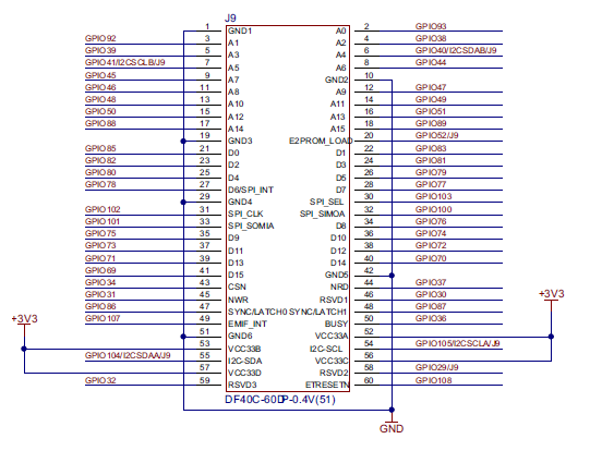
In addtion, can the pin GPIO 72 be the EMIF data transmission channel for which is pull up in the schematic diagram, as the following picture shows. And if yes, does the data transmission function have to be implement by manually turned off the SW?

Best regards,
Ditny.
