This thread has been locked.

If you have a related question, please click the "Ask a related question" button in the top right corner. The newly created question will be automatically linked to this question.

TMS320F28335: ADC Block didn't trigger at an expected value

Part Number: TMS320F28335


Hello friends,

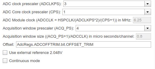
I'm using Ezdsp F28335 ADC function in my project. Here's a simple logic to trigger the GPIO0 when the ADC output is less than 2048 (which is 1.5V).

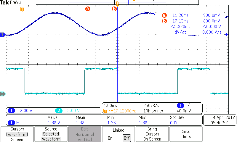
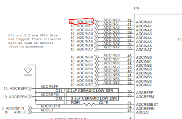
I built it on my target board and test it with a 3 Vpp, 1.5 V offset sine wave voltage input. It triggered at 800 mV, not 1.5 V. I connected the ADCLO to AGRD of DSP. 

I can't figure out why the triggering voltage is 800 mV instead of 1.5V. Could anyone help me figure this problem? 

Thank you very much.

Sincerely,

Xiwen

  • Xiwen,

    Can you provide the settings for the ADC, i.e. ADC Clock, ACQPS as well as how often you have the ADC sampling?  Could you also share the input schematic of the signal to the ADC input?

    My guess is what is happening is that the signal is not being properly sampled; causing the ADC to read 2048 at 800mV.  This is often because the sample and hold capacitor is not properly charged from the input.  

    From the Datasheet http://www.ti.com/product/TMS320F28335/datasheet/specifications#sprs2305090 figure 5-38 we can see that the sample and hold capacitor is 1.64pF.  Assuming you are running at max ADC speed and minimum ACQPS then we have to charge the capacitor in 40ns to at least 99.99%(13 bits) of the input to guarantee the ADC conversion is not impacted by a voltage inaccuracy.

    There are a couple of solutions; you can try to increase the ACQPS until the value stabilizes, you'll need to take into account whatever delay this will introduce into your control loop vs max speed.  Another would be to buffer the input signal with an op-amp such that we can meet the above charge in the min time.

    Let me know if this makes sense, and we can go from here to get the trigger to happen at the correct voltage in your system.

    Best,

    Matthew

  • Hello Matthew,

    Thank you for your suggestion. The input signal is generated from Tektronix AFG2021 Function Generator. I didn't find the schematic of the function generator output side. I tried to increase ACQPS but it doesn't work. Here's the screenshot of my ADC configuration. 

    The sample time is 0.00001. I also mentioned that the floating voltage of ADC is 1.92V when there's no analog input to ADC.

    Can you help me figure it out?

    Thank you very much.

    Sincerely,

    Xiwen

  • I'm sorry. The first picture is wrong. Here is the correct one.

  • Xiwen,
    In the screenshot it is showing ACQ_PS = 4, let's try to max this out and see if there is any difference in behavior. Even if this doesn't get us to ideal we can see if it is helping in the right direction.

    Best,
    Matthew

  • Hello Matthew,

    Thank you for your reply.

    I tried to increase the ACQ_PS from 4 to 15, but it didn't work. The ADC still triggering at 800 mV when I set up the triggering value to be 2048.  I found another problem as well. The floating voltage from ADC becomes 1.9V after I built the Simulink blocks into DSP.

    Can you help me to figure it out? Thank you very much.

    Sincerely,

    Xiwen

  • Xiwen,

    I am not too concerned with the conversion or any voltage observed on the pin of a floating ADC channel.  This is an artifact of the sampling circuit structure and the common mode of some internal nets to the ADC.  Essentially on a floating node we are seeing the sample and hold capacitor transfer its idle state charge out to the pin(or get converted), since there is nothing driving against it if settles to this internal voltage.

    With that said, any amount of drive on the ADC pin will begin to over-ride this voltage with a time component based on the RC of the input itself.  The reason that ACQ_PS increasing should help, is that we are giving the sampling cap longer to "see" the pin voltage when it samples and therefore more time to charge.

    Since increasing did not help, I suspect there is a somewhat large source impedance on the pin.  Just to confirm, you are using the F28335 control card, with the signal from the function generator supplied straight to the ADCINx pin that is being sampled?  Below I've inserted a schematic of just the analog inputs of the Control Card, you can use this to show me where you are inputting your signal from the Tektronix source.

    Best,

    Matthew

  • Hello Matthew,

    I'm using Ezdsp f28335 instead of the control card. I found the schematics in the technical reference book are different from the schematic you provided. I pasted it below. The input signal is given to the ADCINA0 pin  (Pin #2 in the second picture).

    Thanks,

    Xiwen

  • Xiwen,
    Thanks for the update, understand you are using the ezDSP for the 28335. Unlike the control card, there is no native decoupling/sampling capacitor on the ADC inputs. As noted in the schematic the P9 header has VSSA opposite all the ADCINAx channels, so it should be fairly easy to soldier a small capacitor between ADCINA0 and VSS on underside of this header.
    I would start with a 20pF ceramic cap if possible. We should see some immediate improvement to the result after the cap is in place.

    Let me know if you are able to perform the above change to your ezDSP board.

    Best regards,
    Matthew