


Part Number: LAUNCHXL-F28069M
Just a simple question about how the reference guide shows:
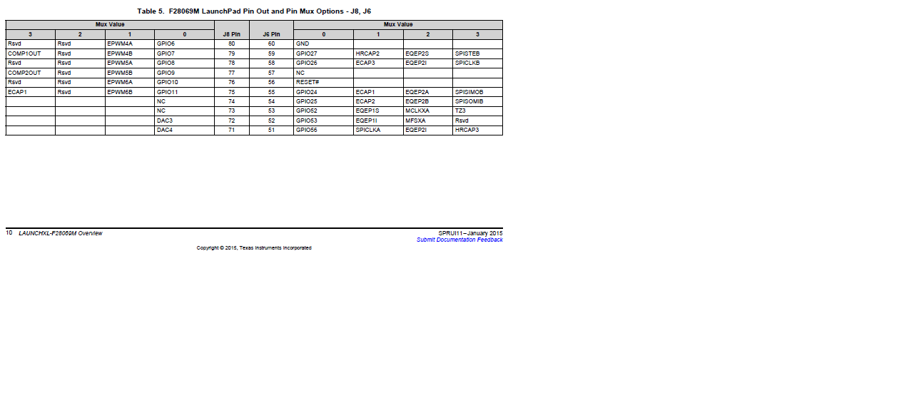
And then GPIO.C shows code like this: Where an example would be GPIO7, and the MUX options dont match up?
GpioCtrlRegs.GPAMUX1.bit.GPIO0 = 1;//p 40 // 0=GPIO 1=EPWM1A 2=rsvd 3=rsvd
GpioCtrlRegs.GPAMUX1.bit.GPIO1 = 0; // 0=GPIO 1=EPWM1B 2=rsvd 3=COMP1OUT
GpioCtrlRegs.GPAMUX1.bit.GPIO2 = 1;//p 38 // 0=GPIO 1=EPWM2A 2=rsvd 3=rsvd
GpioCtrlRegs.GPAMUX1.bit.GPIO3 = 0; // 0=GPIO 1=EPWM2B 2=SPISOMIA 3=COMP2OUT
GpioCtrlRegs.GPAMUX1.bit.GPIO4 = 0; // 0=GPIO 1=EPWM3A 2=rsvd 3=rsvd
GpioCtrlRegs.GPAMUX1.bit.GPIO5 = 3;//p 35 // 0=GPIO 1=EPWM3B 2=SPISIMOA 3=ECAP1
GpioCtrlRegs.GPAMUX1.bit.GPIO6 = 0; // 0=GPIO 1=EPWM4A 2=EPWMSYNCI 3=EPWMSYNCO
GpioCtrlRegs.GPAMUX1.bit.GPIO7 = 0; // 0=GPIO 1=EPWM4B 2=SCIRXDA 3=ECAP2
GpioCtrlRegs.GPAMUX1.bit.GPIO8 = 0; // 0=GPIO 1=EPWM5A 2=rsvd 3=ADCSOCAO
GpioCtrlRegs.GPAMUX1.bit.GPIO9 = 0; // 0=GPIO 1=EPWM5B 2=SCITXDB 3=ECAP3
GpioCtrlRegs.GPAMUX1.bit.GPIO10 = 0; // 0=GPIO 1=EPWM6A 2=rsvd 3=ADCSOCBO
GpioCtrlRegs.GPAMUX1.bit.GPIO11 = 0; // 0=GPIO 1=EPWM6B 2=SCIRXDB 3=ECAP1
GpioCtrlRegs.GPAMUX1.bit.GPIO12 = 0; // 0=GPIO 1=TZ1 2=SCITXDA 3=SPISIMOB
GpioCtrlRegs.GPAMUX1.bit.GPIO13 = 0; // 0=GPIO 1=TZ2 2=rsvd 3=SPISOMIB
GpioCtrlRegs.GPAMUX1.bit.GPIO14 = 0; // 0=GPIO 1=TZ3 2=SCITXDB 3=SPICLKB
GpioCtrlRegs.GPAMUX1.bit.GPIO15 = 0; // 0=GPIO 1=ECAP2 2=SCIRXDB 3=SPISTEB
GpioCtrlRegs.GPAMUX2.bit.GPIO16 = 0; // 0=GPIO 1=SPISIMOA 2=rsvd 3=TZ2
GpioCtrlRegs.GPAMUX2.bit.GPIO17 = 0; // 0=GPIO 1=SPISOMIA 2=rsvd 3=TZ3
GpioCtrlRegs.GPAMUX2.bit.GPIO18 = 0; // 0=GPIO 1=SPICLKA 2=SCITXDB 3=XCLKOUT
GpioCtrlRegs.GPAMUX2.bit.GPIO19 = 2; // 0=GPIO/XCLKIN 1=SPISTEA 2=SCIRXDB 3=ECAP1
GpioCtrlRegs.GPAMUX2.bit.GPIO20 = 0; // 0=GPIO 1=EQEP1A 2=MDXA 3=COMP1OUT
GpioCtrlRegs.GPAMUX2.bit.GPIO21 = 0; // 0=GPIO 1=EQEP1B 2=MDRA 3=COMP2OUT
GpioCtrlRegs.GPAMUX2.bit.GPIO22 = 0; // 0=GPIO 1=EQEP1S 2=MCLKXA 3=SCITXDB
GpioCtrlRegs.GPAMUX2.bit.GPIO23 = 0; // 0=GPIO 1=EQEP1I 2=MFSXA 3=SCIRXDB
GpioCtrlRegs.GPAMUX2.bit.GPIO24 = 0; // 0=GPIO 1=ECAP1 2=EQEP2A 3=SPISIMOB
GpioCtrlRegs.GPAMUX2.bit.GPIO25 = 0; // 0=GPIO 1=ECAP2 2=EQEP2B 3=SPISOMIB
GpioCtrlRegs.GPAMUX2.bit.GPIO26 = 0; // 0=GPIO 1=ECAP3 2=EQEP2I 3=SPICLKB
GpioCtrlRegs.GPAMUX2.bit.GPIO27 = 0;//p3 // 0=GPIO 1=HRCAP2 2=EQEP2S 3=SPISTEB
GpioCtrlRegs.GPAMUX2.bit.GPIO28 = 0; // 0=GPIO 1=SCIRXDA 2=SDAA 3=TZ2 ->J1.3
GpioCtrlRegs.GPAMUX2.bit.GPIO29 = 0; // 0=GPIO 1=SCITXDA 2=SCLA 3=TZ3
GpioCtrlRegs.GPAMUX2.bit.GPIO30 = 0; // 0=GPIO 1=CANRXA 2=EQEP2I 3=EPWM7A
GpioCtrlRegs.GPAMUX2.bit.GPIO31 = 0; // 0=GPIO 1=CANTXA 2=EQEP2S 3=EPWM8A
//--- Group B pins
GpioCtrlRegs.GPBCTRL.all = 0x00000000; // QUALPRD = SYSCLKOUT for all group B GPIO
GpioCtrlRegs.GPBQSEL1.all = 0x00000000; // No qualification for all group B GPIO 32-44
GpioCtrlRegs.GPBQSEL2.all = 0x00000000; // No qualification for all group B GPIO 50-58
GpioCtrlRegs.GPBDIR.all = 0x00000000; // All group B GPIO are inputs
GpioCtrlRegs.GPBPUD.all = 0x00000000; // All group B pullups enabled
GpioCtrlRegs.GPBMUX1.bit.GPIO32 = 0; // 0=GPIO 1=SDAA 2=EPWMSYNCI 3=ADCSOCAO
GpioCtrlRegs.GPBMUX1.bit.GPIO33 = 0; // 0=GPIO 1=SCLA 2=EPWMSYNCO 3=ADCSOCBO
GpioCtrlRegs.GPBMUX1.bit.GPIO34 = 0; // 0=GPIO 1=COMP2OUT 2=rsvd 3=COMP3OUT
GpioCtrlRegs.GPBMUX1.bit.GPIO35 = 0; // 0=GPIO (TDI) 1=rsvd 2=rsvd 3=rsvd
GpioCtrlRegs.GPBMUX1.bit.GPIO36 = 0; // 0=GPIO (TMS) 1=rsvd 2=rsvd 3=rsvd
GpioCtrlRegs.GPBMUX1.bit.GPIO37 = 0; // 0=GPIO (TDO) 1=rsvd 2=rsvd 3=rsvd
GpioCtrlRegs.GPBMUX1.bit.GPIO38 = 0; // 0=GPIO/XCLKIN (TCK) 1=rsvd 2=rsvd 3=rsvd
GpioCtrlRegs.GPBMUX1.bit.GPIO39 = 0; // 0=GPIO 1=rsvd 2=rsvd 3=rsvd
GpioCtrlRegs.GPBMUX1.bit.GPIO40 = 0; // 0=GPIO 1=EPWM7A 2=SCITXDB 3=rsvd
GpioCtrlRegs.GPBMUX1.bit.GPIO41 = 0; // 0=GPIO 1=EPWM7B 2=SCIRXDB 3=rsvd
GpioCtrlRegs.GPBMUX1.bit.GPIO42 = 0; // 0=GPIO 1=EPWM8A 2=TZ1 3=COMP1OUT
GpioCtrlRegs.GPBMUX1.bit.GPIO43 = 0; // 0=GPIO 1=EPWM8B 2=TZ2 3=COMP2OUT
GpioCtrlRegs.GPBMUX1.bit.GPIO44 = 0; // 0=GPIO 1=MFSRA 2=SCIRXDB 3=EPWM7B
GpioCtrlRegs.GPBMUX2.bit.GPIO50 = 0; // 0=GPIO 1=EQEP1A 2=MDXA 3=TZ1
GpioCtrlRegs.GPBMUX2.bit.GPIO51 = 0; // 0=GPIO 1=EQEP1B 2=MDRA 3=TZ2
GpioCtrlRegs.GPBMUX2.bit.GPIO52 = 0; // 0=GPIO 1=EQEP1S 2=MCLKXA 3=TZ3
GpioCtrlRegs.GPBMUX2.bit.GPIO53 = 0; // 0=GPIO 1=EQEP1I 2=MFSXA 3=rsvd
GpioCtrlRegs.GPBMUX2.bit.GPIO54 = 0; // 0=GPIO 1=SPISIMOA 2=EQEP2A 3=HRCAP1
GpioCtrlRegs.GPBMUX2.bit.GPIO55 = 0; // 0=GPIO 1=SPISOMIA 2=EQEP2B 3=HRCAP2
GpioCtrlRegs.GPBMUX2.bit.GPIO56 = 0; // 0=GPIO 1=SPICLKA 2=EQEP2I 3=HRCAP3
GpioCtrlRegs.GPBMUX2.bit.GPIO57 = 0; // 0=GPIO 1=SPISTEA 2=EQEP2S 3=HRCAP4
GpioCtrlRegs.GPBMUX2.bit.GPIO58 = 0; // 0=GPIO 1=MCLKRA 2=SCITXDB 3=EPWM7A
One last quick question: This shows GPIO from 0-58, while the reference guide is missing quite a bit of them. Why might that be?
Thanks!


