


Part Number: TMS320F2812
Hi,
Base on F2812 data sheet, section 6.8 Power Sequencing Requirements option2,
First 3.3V on, then 1.9V ramp,
Other condition: 1.8 V or 1.9 V (V DD /V DD1 ) should not reach 0.3 V until V DDIO has reached 2.5 V.
Power ramp up as below picture, CS pin will have a low state to access FARM when power ramp up.
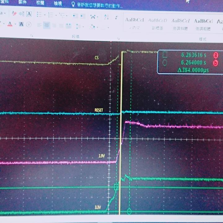
but if 1.9V and 3.3V ramp up together as below picture , CS pin also ramp up high level when power ramp up.
It did not have low state to access FARM incorrectly.

Is it possible that DSP power-on fail when 1.9V and 3.3V ramp up together ?
thanks,
best regards,
Simen
