This thread has been locked.
If you have a related question, please click the "Ask a related question" button in the top right corner. The newly created question will be automatically linked to this question.
Hello! I'm trying to receive a string from an HC06 running at 9600BAUD. I have the same system working on the MSP430F5529.
This is the code that I imagine should be working. My problem is not actually receiving anything in RXBUF. I am getting interrupted which means I am receiving a byte, but nothing is being transferred to my array.
I've tried assuming LSPCLK is at 90MHz, and the default SYSCLK/4, which equates to 22.5MHz. Using the formula:
LSPCLK/(9600*8) - 1, I've found a value of 0x123 FOR 22.5MHz and a value of 0x492 for 90MHz to be stored in:
SciaRegs.SCIHBAUD = 0x0000;
SciaRegs.SCILBAUD = 0x0492; // 9600 BAUD, ive also tried 0x0123.
I must be doing something wrong! If someone could help me, that'd be greatly appreciated as this a small part for a school project!
Thanks!
Heres the code i'm running (the relevant stuff):
__interrupt void sciaRxFifoIsr(void);
char RXParseData[256] = {}; // Array which stores the data received in RXBUF
void main(void)
{
//--- CPU Initialization
InitSysCtrl(); // Initialize the CPU (FILE: SysCtrl.c)
InitPieCtrl(); // Initialize and enable the PIE (FILE: PieCtrl.c)
InitWatchdog(); // Initialize the Watchdog Timer (FILE: WatchDog.c)
//---- SCI -- SETUP
EALLOW;
/* Enable internal pull-up for the selected pins */
// Pull-ups can be enabled or disabled disabled by the user.
// This will enable the pullups for the specified pins.
GpioCtrlRegs.GPAPUD.bit.GPIO28 = 0; // Enable pull-up for GPIO28 (SCIRXDA)
/* Set qualification for selected pins to asynch only */
// Inputs are synchronized to SYSCLKOUT by default.
// This will select asynch (no qualification) for the selected pins.
GpioCtrlRegs.GPAQSEL2.bit.GPIO28 = 3; // Asynch input GPIO28 (SCIRXDA)
/* Configure SCI-A pins using GPIO regs*/
// This specifies which of the possible GPIO pins will be SCI functional pins.
GpioCtrlRegs.GPAMUX2.bit.GPIO28 = 1; // Configure GPIO28 for SCIRXDA operation
EDIS;
// END SCI SETUP
// Step 3. Clear all interrupts and initialize PIE vector table:
// Disable CPU interrupts
DINT;
// Initialize PIE control registers to their default state.
// The default state is all PIE interrupts disabled and flags
// are cleared.
// This function is found in the F2806x_PieCtrl.c file.
InitPieCtrl();
// Disable CPU interrupts and clear all CPU interrupt flags:
IER = 0x0000;
IFR = 0x0000;
// Initialize the PIE vector table with pointers to the shell Interrupt
// Service Routines (ISR).
// This will populate the entire table, even if the interrupt
// is not used in this example. This is useful for debug purposes.
// The shell ISR routines are found in F2806x_DefaultIsr.c.
// This function is found in F2806x_PieVect.c.
InitPieVectTable();
// Interrupts that are used in this example are re-mapped to
// ISR functions found within this file.
EALLOW; // This is needed to write to EALLOW protected registers
PieVectTable.SCIRXINTA = &sciaRxFifoIsr;
EDIS; // This is needed to disable write to EALLOW protected registers
//FIFO SETUP
SciaRegs.SCICCR.all =0x0007; // 1 stop bit, No loopback
// No parity,8 char bits,
// async mode, idle-line protocol
SciaRegs.SCICTL1.all =0x0001; // enable RX, internal SCICLK,
// Disable TX, RX ERR, SLEEP, TXWAKE
SciaRegs.SCICTL2.bit.RXBKINTENA =1;
SciaRegs.SCIHBAUD = 0x0000;
SciaRegs.SCILBAUD = 0x0492; // 9600 BAUD, ive also tried 0x0123.
SciaRegs.SCIFFRX.all=0x0022;
SciaRegs.SCIFFCT.all=0x00;
SciaRegs.SCICTL1.all =0x0021; // Relinquish SCI from Reset
SciaRegs.SCIFFRX.bit.RXFIFORESET=1;
// Enable interrupts required for this example
PieCtrlRegs.PIECTRL.bit.ENPIE = 1; // Enable the PIE block
PieCtrlRegs.PIEIER9.bit.INTx1=1; // PIE Group 9, INT1
PieCtrlRegs.PIEIER9.bit.INTx2=1; // PIE Group 9, INT2
IER = 0x100; // Enable CPU INT
EINT;
//--- Enable global interrupts
asm(" CLRC INTM, DBGM"); // Enable global interrupts and realtime debug
}
__interrupt void sciaRxFifoIsr(void)
{
Uint16 i = 0;
while(1)
{
RXParseData[i]=SciaRegs.SCIRXBUF.all;
i++;
}
SciaRegs.SCIFFRX.bit.RXFFOVRCLR=1; // Clear Overflow flag
SciaRegs.SCIFFRX.bit.RXFFINTCLR=1; // Clear Interrupt flag
PieCtrlRegs.PIEACK.all|=0x100; // Issue PIE ack
}
Unfortunately, this did not resolve the issue. And yes, you are understanding the problem correctly!
ISR change:
__interrupt void sciaRxFifoIsr(void)
{
Uint16 i = 0;
PieCtrlRegs.PIEACK.all|=0x100; // Issue PIE ack
while(1)
{
RXParseData[i]=SciaRegs.SCIRXBUF.all; // Read data
i++;
}
SciaRegs.SCIFFRX.bit.RXFFOVRCLR=1; // Clear Overflow flag
SciaRegs.SCIFFRX.bit.RXFFINTCLR=1; // Clear Interrupt flag
}
After some thought, I'm questioning my hardware set up. Right now, I have the TX of the HC06 connected to PIN 3 of the C2000. I have both jumpers on JP6 & JP7. Could this be a problem?
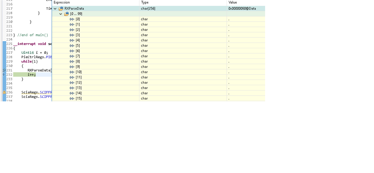
I have a fairly good understanding of UART, so i'd just like to ask: if I'm receiving an interrupt but nothing is being transferred to my array, how could I be receiving the interrupt? Wouldn't this be at least seen as a start bit, followed by eight 0's and then a stop bit? Would the array show 0's or simply just '.' as shown here (i = 9 @ the time of this screencap, after I sent the message 'Route 1'):
Andrew,
Now, the way you have written this while(1) loop in your ISR will cause your buffer to flood with 'data'. The array will fill indiscriminately of if you have data in the RXBUF. Because you have received an interrupt I would have expected that the first few array elements should have had values.(that is weird)Now I have never read from the RX buffer as fast as the device would let me before, so I honestly don't know what 'data' it would fill the buffer with assuming there were no values in the RXBUF. Occasionally yes you would receive a value in the buffer and that would be transferred to the array, but it would be overwritten at some point.
I recommend that you read from the RXFFST registers and then decide how many words you would like to pull out of the FIFO. As you read the words you can put them into an array if you would like, but after that you should acknowledge the interrupt and return from the ISR.
Forgive me if I missed any of this information in the posts above.
Regards,
Cody
Hey Cody!
Do you think it'd be easier to just set LSPCLK to a frequency instead of measuring it? I recently went to check its frequency but I got a little confused by the registers. I didn't spend too much time on it because I'm just so busy with this project and my other courses. If we can just set it to SYSCLK/4, that'd be great! Would you be able to provide code for it?
I have confirmed that HC06 is sending the right data. I also had this same system originally on an MSP430.
I have the TX of the HC06 going to PIN 3 on the launchpad which is set as GPIO28 because I have JP6 and JP7 jumpers on. (I believe this is correct)
I know the ISR while loop isn't right. That was just to debug the program. I am setting a break point and immediately going in there and checking the data, but the data isn't showing up! I've also used an 'if I detect a null' but that would also break (I believe it ended up being a forever loop).
I checked into the RXFFST registers, but I will be receiving a maximum of 4 unique strings (GO, STOP, Route 1, and Route 2) at very long time intervals. I feel like using the FIFO peripheral will be a hassle as I just need a simple receiving program to read a few characters to parse. I originally looked into that, but I felt like I'd be configuring the registers to not use them.
Oops, Sorry! When I sent this on my partners computer, it didn't show up! Also, it didn't show up until after I sent the message I just sent!... They both say the same thing!
Andrew,
Sorry Andrew, I can't provide code without a significant amount of legalities. Configuring XCLKOUT is very easy though...select XCLKOUT on GPIO18's MUX configuration, then ensure you are using the correct dividers( see figure 1.4.2.11 "XCLKOUT Generation" in the TRM) and check that you see the clock rate you expect on GPIO18.
If you didn't want to use the FIFOs why do you have them configured(see quote below)? You should use the FIFO, the code you started from already configures them so it shouldn't be any extra work.
Andrew Wenaus said:SciaRegs.SCIFFRX.all=0x0022;
I would also recommend that you create a standard communication language, there is no need to make it human readable "ROUTE 1" and "GO" could be coded into a shorter message like "R1" and "C1" where the number following an R is a route selection and the number following a C is a command (0= stop, 1= go,2= idle,3= victory dance, etc.) It will speed things up!
Yes, having a jumper on JP6 and JP7 is likely an issue, the schematic states that this is "UART Disable". If you want to use UART on GPIO28 and GPIO29 then you should configure MUX_SEL=0 and CH_SEL=1. The selection of MUX_SEL and CH_SEL is done with JP6/JP7 and is fully described on Page 6 of the schematic. The schematic(LAUNCHXL-F28069M_sch.pdf) can be found in both C2000Ware and controlSuite.
We have all faced a seemingly insurmountable set of tasks, think of it as a time of growth and it will be.
Hope it helps!
Regards,
Cody
OK, we will mark this a complete and continue the debug in the new thread.
CCS/LAUNCHXL-F28069M: Unable to Receive UART data - C2000 microcontrollers forum - C2000™︎ microcontrollers...
Regards,
Cody