This thread has been locked.

If you have a related question, please click the "Ask a related question" button in the top right corner. The newly created question will be automatically linked to this question.

CCS/LAUNCHXL-F28069M: I²C issue with 24C04 E²PROM

Part Number: LAUNCHXL-F28069M
Other Parts Discussed in Thread: CONTROLSUITE

Tool/software: Code Composer Studio

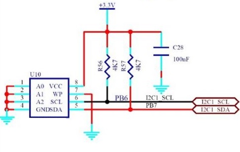
I need to use LAUNCHXL-F28069's I²C communication interface (asynch input GPIO32 (SDAA) and asynch input GPIO33 (SCLA)) to read and write my non-volatile parameters from/to 24C04 e²prom. I have used the same connection circuit below for 24C04.


VCC is 3.3V because its datasheet says VCC=1.8V to 5.5V. +3.3V and ground connections are from my launchxl kit. Not from a different source.

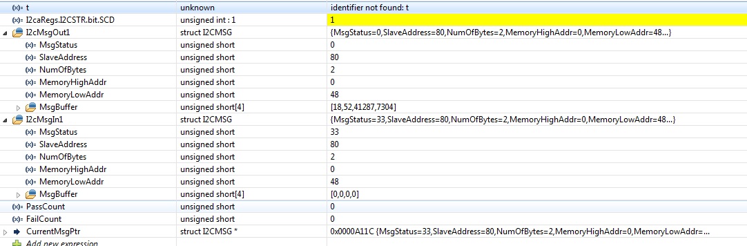
I have used the example on the attachment.

But my code is stuck here :

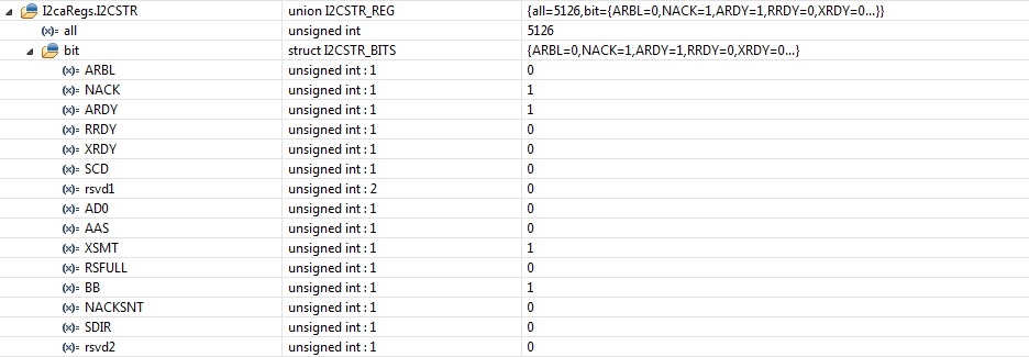
And my I2caRegs.I2CSTR status registers are like that :

I am new about i²c configuration and I think I read the eeprom 1 time but shouldn't I read it continuously? What is wrong with XSMT or SCD bits? Thanks for your attention.

//#############################################################################
//
//  File:   f2802x_examples_ccsv4/i2c_eeprom/Example_F2802xI2c_eeprom.c
//
//  Title:  F2802x I2C EEPROM Example
//
//  Group:          C2000
//  Target Device:  TMS320F2802x
//
//! \addtogroup example_list
//!  <h1>I2C EEPROM</h1>
//!
//!   This program will write 1-14 words to EEPROM and read them back.
//!   The data written and the EEPROM address written to are contained
//!   in the message structure, I2cMsgOut1. The data read back will be
//!   contained in the message structure I2cMsgIn1.
//!
//!   This program will work with the on-board I2C EEPROM supplied on
//!   the F2802x eZdsp or another EEPROM connected to the devices I2C bus
//!   with a slave address of 0x50
//
//  (C) Copyright 2012, Texas Instruments, Inc.
//#############################################################################
// $TI Release: f2802x Support Library v210 $
// $Release Date: Mon Sep 17 09:13:31 CDT 2012 $
//#############################################################################

#include "DSP28x_Project.h"     // Device Headerfile and Examples Include File

// Note: I2C Macros used in this example can be found in the
// DSP2802x_I2C_defines.h file

// Prototype statements for functions found within this file.
void I2CA_Init(void);
Uint16 ReadEeprom(Uint16 e2promaddress);
void WriteEeprom(Uint16 e2promaddress, Uint16 data);


Uint32 DataRead[256];//] = { 0,0,0,0,0,0,0,0,0,0};

void main(void)
{

// Step 1. Initialize System Control:
// PLL, WatchDog, enable Peripheral Clocks
// This example function is found in the DSP2802x_SysCtrl.c file.
   InitSysCtrl();

// Step 2. Initalize GPIO:
// This example function is found in the DSP2802x_Gpio.c file and
// illustrates how to set the GPIO to it's default state.
// InitGpio();
// Setup only the GP I/O only for I2C functionality
   InitI2CGpio(); // using GPIO 32 and 33

// Step 3. Clear all interrupts and initialize PIE vector table:
// Disable CPU interrupts
   DINT;

// Initialize PIE control registers to their default state.
// The default state is all PIE interrupts disabled and flags
// are cleared.
// This function is found in the DSP2802x_PieCtrl.c file.
   InitPieCtrl();

// Disable CPU interrupts and clear all CPU interrupt flags:
   IER = 0x0000;
   IFR = 0x0000;

   // If running from flash copy RAM only functions to RAM
#ifdef _FLASH
   memcpy(&RamfuncsRunStart, &RamfuncsLoadStart, (size_t)&RamfuncsLoadSize);
#endif

// Initialize the PIE vector table with pointers to the shell Interrupt
// Service Routines (ISR).
// This will populate the entire table, even if the interrupt
// is not used in this example.  This is useful for debug purposes.
// The shell ISR routines are found in DSP2802x_DefaultIsr.c.
// This function is found in DSP2802x_PieVect.c.
   InitPieVectTable();


   // Step 4. Initialize all the Device Peripherals:
   // This function is found in DSP2802x_InitPeripherals.c
   // InitPeripherals(); // Not required for this example
      I2CA_Init();
      DELAY_US(100);
   // Step 5. User specific code

      EINT;

   unsigned int j;
   j =0;

   // Application loop
   for(;;)
   {
	   //WriteEeprom(j, 10+j);
	   //WriteEeprom(j+1, 10+j+1);

	   DataRead[j] = ReadEeprom(j);
	   //DataRead[j+1] = (ReadEeprom(j+1) << 8) | DataRead[j] ;
	   DataRead[j+1] = ReadEeprom(j+1) ;

	   j=j+2;

	   if (j>=200)
		   j = 0;

   }   // end of for(;;)
}   // end of main

void I2CA_Init(void)
{
		I2caRegs.I2CMDR.all 	= 0x0000;
	   // Initialize I2C
	   I2caRegs.I2CSAR = 0x0050;        // Slave address - EEPROM control code

	   // I2CCLK = SYSCLK/(I2CPSC+1)
	   #if (CPU_FRQ_40MHZ||CPU_FRQ_50MHZ)
	     I2caRegs.I2CPSC.all = 4;       // Prescaler - need 7-12 Mhz on module clk
	   #endif

	   #if (CPU_FRQ_60MHZ)
	     I2caRegs.I2CPSC.all = 5;  //6     // Prescaler - need 7-12 Mhz on module clk
	   #endif
	   I2caRegs.I2CCLKL = 10;        	// NOTE: must be non zero
	   I2caRegs.I2CCLKH = 5;         	// NOTE: must be non zero
//	   I2caRegs.I2CIER.all = 0x24;      // Enable SCD & ARDY interrupts

	   I2caRegs.I2CMDR.all = 0x0020;    // Take I2C out of reset
	                                    // Stop I2C when suspended

	   I2caRegs.I2CFFTX.all = 0x6000;   // Enable FIFO mode and TXFIFO
	   I2caRegs.I2CFFRX.all = 0x2040;   // Enable RXFIFO, clear RXFFINT,


   return;
}


Uint16 ReadEeprom(Uint16 e2promaddress)
{
	Uint16 addresslow;
	Uint16 addresshigh;
	Uint16 tempdata;

	I2caRegs.I2CMDR.bit.IRS = 1; 				// reset I2C
	while (I2caRegs.I2CSTR.bit.BB == 1);		// busy loop
	I2caRegs.I2CSTR.bit.SCD = 1;				// Clear the SCD bit (stop condition bit)
	while(I2caRegs.I2CMDR.bit.STP == 1);		// stop bit loop

	addresshigh			= e2promaddress>>8;
	addresslow			= e2promaddress;
	I2caRegs.I2CSAR 	= 0x0050;

	while (I2caRegs.I2CSTR.bit.BB == 1);
	I2caRegs.I2CMDR.all = 0x2620;				// start, no stop bit, master, tx, reset I2C
	I2caRegs.I2CCNT		= 0x0002;
	I2caRegs.I2CDXR		= addresshigh;
	I2caRegs.I2CDXR		= addresslow;
	while(!I2caRegs.I2CSTR.bit.ARDY);			// all ready?

	I2caRegs.I2CMDR.all = 0x2C20;				// start, stop bit when CNT =0, master, rx, reset I2C
	I2caRegs.I2CCNT		= 1;

	if(I2caRegs.I2CSTR.bit.NACK == 1)
	{
		 I2caRegs.I2CSTR.all = I2C_CLR_NACK_BIT; 	// 0x0002
	}
	I2caRegs.I2CMDR.bit.STP = 1;					// stop bit when CNT=0

	while(!I2caRegs.I2CSTR.bit.SCD);				// stop bit detected?

	//tempdata	= I2caRegs.I2CDRR << 8; 			// read data
	tempdata	= I2caRegs.I2CDRR;

	DELAY_US(100);

	return(tempdata);
}


void WriteEeprom(Uint16 e2promaddress, Uint16 data)
{
	Uint16 addresslow;
	Uint16 addresshigh;

	I2caRegs.I2CMDR.bit.IRS = 1; 			// reset I2C

	addresshigh			= (e2promaddress>>8)&0x00FF;
	addresslow			= e2promaddress&0x00FF;
	I2caRegs.I2CSAR 	= 0x0050;			// EEPROM control bits + address (A0-A2). for 24LC256, 0 1 0 1 0 A0 A1 A2

	while (I2caRegs.I2CSTR.bit.BB == 1);

	I2caRegs.I2CCNT		= 3	;
	I2caRegs.I2CMDR.all = 0x6E20; 				//start, stop, no rm, reset i2c
	I2caRegs.I2CDXR		= addresshigh;
	I2caRegs.I2CDXR		= addresslow;
//	I2caRegs.I2CDXR		= (data >> 8) & 0x00FF;	// high byte data
	I2caRegs.I2CDXR		= data;					// low byte data
	I2caRegs.I2CMDR.bit.STP = 1;  				// stop bit when CNT=0

	while(!I2caRegs.I2CSTR.bit.SCD);			// stop bit detected?

	DELAY_US(5000);								// 5ms = write cycle time of 24LC256 - based on datasheet 24LC256

	return;
}

//===========================================================================
// No more.
//===========================================================================

  • Hi there John,

    Can you tell me if you see the I2C signals on the LaunchPad?
    Did you receive a NACK and it was cleared before getting stuck?

    one additional thing, you mention that you are using the F28069M launchPad, but are using code originally written for the F2802x. These devices, run at differeny SYSCLK frequencies. Please check on your SYSCLK frequency configuration and ensure that the internal I2C clock dividers are set up such that the I2C clock prescalers divide down the input clock (SYSCLK) to between 7 and 12 MHz.

    Thanks,
    Mark
  • Hello Mr. Labbato,

    "Can you tell me if you see the I2C signals on the LaunchPad? "

    32 and 33 pins show me only 3.3V on my oscilloscope.

    "Did you receive a NACK and it was cleared before getting stuck?"

    Aye. Below :

    " you mention that you are using the F28069M launchPad, but are using code originally written for the F2802x. These devices, run at differeny SYSCLK frequencies.  Please check on your SYSCLK frequency configuration and  ensure that the internal I2C clock dividers are set up such that  the I2C clock prescalers divide down the input clock (SYSCLK)  to between 7 and 12 MHz."

    Code flow for F28069 is the same but I didn't check I2C clock. Thank you, I will check. 

  • Please let me know the results of the clock configuration as you get to it. If that is not correct, the I2C is not guaranteed to operate properly.

    Thanks,
    Mark
  • oid I2CA_Init(void)
    {
            I2caRegs.I2CMDR.all     = 0x0000;
           // Initialize I2C
           I2caRegs.I2CSAR = 0x0050;        // Slave address - EEPROM control code
    
           // I2CCLK = SYSCLK/(I2CPSC+1)
    
             I2caRegs.I2CPSC.all = 6;  //6     // Prescaler - need 7-12 Mhz on module clk
    
    
           I2caRegs.I2CCLKL = 10;           // NOTE: must be non zero
           I2caRegs.I2CCLKH = 5;            // NOTE: must be non zero
    //     I2caRegs.I2CIER.all = 0x24;      // Enable SCD & ARDY interrupts
    
           I2caRegs.I2CMDR.all = 0x0020;    // Take I2C out of reset
                                            // Stop I2C when suspended
    
           I2caRegs.I2CFFTX.all = 0x6000;   // Enable FIFO mode and TXFIFO
           I2caRegs.I2CFFRX.all = 0x2040;   // Enable RXFIFO, clear RXFFINT,
    
    
       return;
    }

    I have also tried "Example_2806xI2C_eeprom" example in which its F2806x_CpuTimers.c is like below :

    //###########################################################################
    //
    // FILE:	F2806x_CpuTimers.c
    //
    // TITLE:	CPU 32-bit Timers Initialization & Support Functions.
    //
    // NOTES:
    //
    //###########################################################################
    // $TI Release: F2806x C/C++ Header Files and Peripheral Examples V151 $
    // $Release Date: February  2, 2016 $
    // $Copyright: Copyright (C) 2011-2016 Texas Instruments Incorporated -
    //             http://www.ti.com/ ALL RIGHTS RESERVED $
    //###########################################################################
    
    #include "F2806x_Device.h"     // Headerfile Include File
    #include "F2806x_Examples.h"   // Examples Include File
    
    
    struct CPUTIMER_VARS CpuTimer0;
    struct CPUTIMER_VARS CpuTimer1;
    struct CPUTIMER_VARS CpuTimer2;
    
    //---------------------------------------------------------------------------
    // InitCpuTimers:
    //---------------------------------------------------------------------------
    // This function initializes all three CPU timers to a known state.
    //
    void InitCpuTimers(void)
    {
        // CPU Timer 0
    	// Initialize address pointers to respective timer registers:
    	CpuTimer0.RegsAddr = &CpuTimer0Regs;
    	// Initialize timer period to maximum:
    	CpuTimer0Regs.PRD.all  = 0xFFFFFFFF;
    	// Initialize pre-scale counter to divide by 1 (SYSCLKOUT):
    	CpuTimer0Regs.TPR.all  = 0;
    	CpuTimer0Regs.TPRH.all = 0;
    	// Make sure timer is stopped:
    	CpuTimer0Regs.TCR.bit.TSS = 1;
    	// Reload all counter register with period value:
    	CpuTimer0Regs.TCR.bit.TRB = 1;
    	// Reset interrupt counters:
    	//CpuTimer0.InterruptCount = 0;
    
    
    // Initialize address pointers to respective timer registers:
    	CpuTimer1.RegsAddr = &CpuTimer1Regs;
    	CpuTimer2.RegsAddr = &CpuTimer2Regs;
    	// Initialize timer period to maximum:
    	CpuTimer1Regs.PRD.all  = 0xFFFFFFFF;
    	CpuTimer2Regs.PRD.all  = 0xFFFFFFFF;
        // Initialize pre-scale counter to divide by 1 (SYSCLKOUT):
    	CpuTimer1Regs.TPR.all  = 0;
    	CpuTimer1Regs.TPRH.all = 0;
    	CpuTimer2Regs.TPR.all  = 0;
    	CpuTimer2Regs.TPRH.all = 0;
        // Make sure timers are stopped:
    	CpuTimer1Regs.TCR.bit.TSS = 1;
    	CpuTimer2Regs.TCR.bit.TSS = 1;
    	// Reload all counter register with period value:
    	CpuTimer1Regs.TCR.bit.TRB = 1;
    	CpuTimer2Regs.TCR.bit.TRB = 1;
    	// Reset interrupt counters:
    	//CpuTimer1.InterruptCount = 0;
    	//CpuTimer2.InterruptCount = 0;
    
    }
    
    //---------------------------------------------------------------------------
    // ConfigCpuTimer:
    //---------------------------------------------------------------------------
    // This function initializes the selected timer to the period specified
    // by the "Freq" and "Period" parameters. The "Freq" is entered as "MHz"
    // and the period in "uSeconds". The timer is held in the stopped state
    // after configuration.
    //
    void ConfigCpuTimer(struct CPUTIMER_VARS *Timer, float Freq, float Period)
    {
    	Uint32 	PeriodInClocks;
    
    	// Initialize timer period:
    	Timer->CPUFreqInMHz = Freq;
    	Timer->PeriodInUSec = Period;
    	PeriodInClocks = (long) (Freq * Period);
    	Timer->RegsAddr->PRD.all = PeriodInClocks - 1; // Counter decrements PRD+1 times each period
    
    	// Set pre-scale counter to divide by 1 (SYSCLKOUT):
    	Timer->RegsAddr->TPR.all  = 0;
    	Timer->RegsAddr->TPRH.all  = 0;
    
    	// Initialize timer control register:
    	Timer->RegsAddr->TCR.bit.TSS = 1;      // 1 = Stop timer, 0 = Start/Restart Timer
    	Timer->RegsAddr->TCR.bit.TRB = 1;      // 1 = reload timer
    	Timer->RegsAddr->TCR.bit.SOFT = 0;
    	Timer->RegsAddr->TCR.bit.FREE = 0;     // Timer Free Run Disabled
    	Timer->RegsAddr->TCR.bit.TIE = 1;      // 0 = Disable/ 1 = Enable Timer Interrupt
    
    	// Reset interrupt counter:
    	Timer->InterruptCount = 0;
    
    }
    
    //===========================================================================
    // End of file.
    //===========================================================================
    

    When I debug C:\ti\controlSUITE\device_support\f2806x\v151\F2806x_examples_ccsv5\i2c_eeprom, nothing happens. Oscilloscope shows +3V3 on both SDAA and SCLA pins.

    C:\ti\controlSUITE\device_support\f2806x\v150\F2806x_examples_ccsv5\i2c_eeprom is a bit more enthusiastic. :D Nothing happens on SDAA and SCLA but at least D7 led on the launchxl blinks. :)

  • Troodon,

    What are you trying to say with the shared the code and screenshots? Does the example work now?

    -Mark
  • No.
    +3.3V and ground connections are from my launchxl kit and I think that is the problem. I will supply the 24c04 with a different source. I haven't seen any communication or clock signal on the oscilloscope so NACK is activated all the time.

  • I still haven't solved the problem.

    I2cMsgIn1.MsgStatus is usually 33 (decimal) and sometimes 32 (decimal).

    I2cMsgIn1.MsgBuffer[0], I2cMsgIn1.MsgBuffer[1], I2cMsgIn1.MsgBuffer[2], I2cMsgIn1.MsgBuffer[3] are "0" 

    On the other hand;

    I2cMsgOut1.MsgBuffer[0] = 18

    I2cMsgOut1.MsgBuffer[1] = 52

    I2cMsgOut1.MsgBuffer[2] = 42092

    I2cMsgOut1.MsgBuffer[3] = 6940

    I2C  Message Commands for I2CMSG struct (C:\ti\controlSUITE\device_support\f2806x\v151\F2806x_common\include\F2806x_I2c_defines.h) are given below  :

    #define I2C_MSGSTAT_INACTIVE          0x0000
    #define I2C_MSGSTAT_SEND_WITHSTOP     0x0010
    #define I2C_MSGSTAT_WRITE_BUSY        0x0011
    #define I2C_MSGSTAT_SEND_NOSTOP       0x0020
    #define I2C_MSGSTAT_SEND_NOSTOP_BUSY  0x0021
    #define I2C_MSGSTAT_RESTART           0x0022
    #define I2C_MSGSTAT_READ_BUSY         0x0023

    These are hex values so 32 means "I2C_MSGSTAT_SEND_NOSTOP" and 33 means "I2C_MSGSTAT_SEND_NOSTOP_BUSY"

    Again,

    the project is C:\ti\controlSUITE\device_support\f2806x\v151\F2806x_examples_ccsv5\i2c_eeprom

    compiler version is TI v16.9.3.LTS

    When I use "Step In (F5)", there is a loop here.

    //////////////////////////////////
          // Write data to EEPROM section //
          //////////////////////////////////
    
          // Check the outgoing message to see if it should be sent.
          // In this example it is initialized to send with a stop bit.
          if(I2cMsgOut1.MsgStatus == I2C_MSGSTAT_SEND_WITHSTOP)
          {
             Error = I2CA_WriteData(&I2cMsgOut1);
             // If communication is correctly initiated, set msg status to busy
             // and update CurrentMsgPtr for the interrupt service routine.
             // Otherwise, do nothing and try again next loop. Once message is
             // initiated, the I2C interrupts will handle the rest. Search for
             // i2c_int1a_isr in this file.
             if (Error == I2C_SUCCESS)
             {
                CurrentMsgPtr = &I2cMsgOut1;
                I2cMsgOut1.MsgStatus = I2C_MSGSTAT_WRITE_BUSY;
             }
          }  // end of write section
    
          ///////////////////////////////////
          // Read data from EEPROM section //
          ///////////////////////////////////
    
          // Check outgoing message status. Bypass read section if status is
          // not inactive.
          if (I2cMsgOut1.MsgStatus == I2C_MSGSTAT_INACTIVE)
          {
             // Check incoming message status.
             if(I2cMsgIn1.MsgStatus == I2C_MSGSTAT_SEND_NOSTOP)
             {
                // EEPROM address setup portion
                while(I2CA_ReadData(&I2cMsgIn1) != I2C_SUCCESS)
                {
                   // Maybe setup an attempt counter to break an infinite while
                   // loop. The EEPROM will send back a NACK while it is performing
                   // a write operation. Even though the write communique is
                   // complete at this point, the EEPROM could still be busy
                   // programming the data. Therefore, multiple attempts are
                   // necessary.
                }
                // Update current message pointer and message status
                CurrentMsgPtr = &I2cMsgIn1;
                I2cMsgIn1.MsgStatus = I2C_MSGSTAT_SEND_NOSTOP_BUSY;
             }

    Because "I2cMsgOut1.MsgStatus" is "17" which is "I2C_MSGSTAT_WRITE_BUSY".

    After a while or after "F7 Step Return", I2cMsgOut1.MsgStatus becomes 0, I2C_MSGSTAT_INACTIVE.

  • Troodoon,

    Assuming your configuration code has not changed since this reply: (https://e2e.ti.com/support/microcontrollers/c2000/f/171/p/684501/2523457#2523457 ), your I2C is attempting to run at 514.285 KHz, which is not compatible with the I2C specification. The I2C module clock is also above the 12 MHz maximum as specified in the Datasheet. Adjust I2CPS to get the I2C module clock to be between 7 and 12 MHz: I2CPS = 8 should be good, as the I2C module clock will be 10 MHz, right in the required range.

    You will need to also ensure I2CCLKCL and I2CCLKH registers to get the master clock rate at or below 400 KHz. with your current setting of 10 and 5, you will get exactly 400 KHz.

    That loop that you mention in your latest post is showing that the EEPROM has not completed it's write cycle. for my EEPROM, this can take a few milliseconds. are you waiting long enough to allow the EEPROM write cycle to happen before flagging any error?

    Using an oscilloscope will help us debug this. Please show some captures from a scope or logic analyzer. This is the sequence of the i2c-eeprom example when writing and then reading 4 words at a time. a log file from an I2C bus analyzer is attached showing each transaction.

    1. Master Write starting address
    2. Master Write 4 bytes of data,
    3. Master Write starting address
    4. Slave NAK during write cycle (repeat for 2.5ms),
    5. Slave ACK the Address write from Master
    6. Master Write starting address
    7. Master Read 4 data bytes
    8. data pass if match.

    I hope this helps clear some confusion up. Please let me know.

    -Mark

    /cfs-file/__key/communityserver-discussions-components-files/171/i2c_5F00_eeprom_2D00_4byte_2D00_example.csv

  • Hello Mr. Labbato,

    Thank you for your answer. 

    I have changed I2CPS as "8".  I2CCLKCL and I2CCLKH are 10 and 5 as you know.

    "are you waiting long enough to allow the EEPROM write cycle to happen before flagging any error?" 

    I just use "C:\ti\controlSUITE\device_support\f2806x\v151\F2806x_examples_ccsv5\i2c_eeprom" example. I haven't changed anything, at least intentionally. I just want to see how example and eeprom i2c communication works. 

    My circuit is below. Sorry for the mess. :)

    Which is : 

    Example's files are on the attachment, seperately.

    When I check "GpioDataRegs.GPADAT.bit.GPIO28 and 29, these changes as 0 or 1 continuously, which is cool.

    But on the oscilloscope, (Autoset) GPIO28 and 29 is like below:

    And check this :

    I don't know if that led inside the circle is relevant with I2C but that gives me the idea that there is a communication. Also I2caRegs.I2CSTR's BB (bus busy) bit is usually 1.

    But as I mentioned, I could not read, and I could not write. 

    When I work with different projects inside the workspace, I think I changed some files like "F2806x_SysCtrl. c". In case of an important difference between the default example and my example project, I added these as txt files one by one. 

    //###########################################################################
    //
    //!  \addtogroup f2806x_example_list
    //!  <h1>I2C EEPROM(i2c_eeprom)</h1>
    //!
    //!  This program requires an external I2C EEPROM connected to
    //!  the I2C bus at address 0x50.
    //!  This program will write 1-14 words to EEPROM and read them back.
    //!  The data written and the EEPROM address written to are contained
    //!  in the message structure, \b I2cMsgOut1. The data read back will be
    //!  contained in the message structure \b I2cMsgIn1.
    //!
    //!  \note This program will only work on kits that have an on-board I2C EEPROM.
    //!
    //!  \b Watch \b Variables \n
    //!  - I2cMsgIn1
    //!  - I2cMsgOut1
    //
    //###########################################################################
    // $TI Release: F2806x C/C++ Header Files and Peripheral Examples V151 $
    // $Release Date: February  2, 2016 $
    // $Copyright: Copyright (C) 2011-2016 Texas Instruments Incorporated -
    //             http://www.ti.com/ ALL RIGHTS RESERVED $
    //###########################################################################
    
    #include "DSP28x_Project.h"     // Device Headerfile and Examples Include File
    
    // Note: I2C Macros used in this example can be found in the
    // F2806x_I2C_defines.h file
    
    // Prototype statements for functions found within this file.
    void   I2CA_Init(void);
    Uint16 I2CA_WriteData(struct I2CMSG *msg);
    Uint16 I2CA_ReadData(struct I2CMSG *msg);
    __interrupt void i2c_int1a_isr(void);
    void pass(void);
    void fail(void);
    
    #define I2C_SLAVE_ADDR        0x50
    #define I2C_NUMBYTES          2
    #define I2C_EEPROM_HIGH_ADDR  0x00
    #define I2C_EEPROM_LOW_ADDR   0x30
    
    // Global variables
    // Two bytes will be used for the outgoing address,
    // thus only setup 14 bytes maximum
    struct I2CMSG I2cMsgOut1={I2C_MSGSTAT_SEND_WITHSTOP,
                              I2C_SLAVE_ADDR,
                              I2C_NUMBYTES,
                              I2C_EEPROM_HIGH_ADDR,
                              I2C_EEPROM_LOW_ADDR,
                              0x12,                   // Msg Byte 1
                              0x34};                  // Msg Byte 2
    
    struct I2CMSG I2cMsgIn1={ I2C_MSGSTAT_SEND_NOSTOP,
                              I2C_SLAVE_ADDR,
                              I2C_NUMBYTES,
                              I2C_EEPROM_HIGH_ADDR,
                              I2C_EEPROM_LOW_ADDR};
    
    struct I2CMSG *CurrentMsgPtr;				// Used in interrupts
    Uint16 PassCount;
    Uint16 FailCount;
    Uint16 Error;
    
    void main(void)
    {
    
       Uint16 i;
    
       CurrentMsgPtr = &I2cMsgOut1;
    
    // Step 1. Initialize System Control:
    // PLL, WatchDog, enable Peripheral Clocks
    // This example function is found in the F2806x_SysCtrl.c file.
       InitSysCtrl();
    
    // Step 2. Initalize GPIO:
    // This example function is found in the F2806x_Gpio.c file and
    // illustrates how to set the GPIO to it's default state.
    // InitGpio();
    // Setup only the GP I/O only for I2C functionality
       InitI2CGpio();
    
    // Step 3. Clear all interrupts and initialize PIE vector table:
    // Disable CPU interrupts
       DINT;
    
    // Initialize PIE control registers to their default state.
    // The default state is all PIE interrupts disabled and flags
    // are cleared.
    // This function is found in the F2806x_PieCtrl.c file.
       InitPieCtrl();
    
    // Disable CPU interrupts and clear all CPU interrupt flags:
       IER = 0x0000;
       IFR = 0x0000;
    
    // Initialize the PIE vector table with pointers to the shell Interrupt
    // Service Routines (ISR).
    // This will populate the entire table, even if the interrupt
    // is not used in this example.  This is useful for debug purposes.
    // The shell ISR routines are found in F2806x_DefaultIsr.c.
    // This function is found in F2806x_PieVect.c.
       InitPieVectTable();
    
    // Interrupts that are used in this example are re-mapped to
    // ISR functions found within this file.
       EALLOW;	// This is needed to write to EALLOW protected registers
       PieVectTable.I2CINT1A = &i2c_int1a_isr;
       EDIS;   // This is needed to disable write to EALLOW protected registers
    
    // Step 4. Initialize all the Device Peripherals:
    // This function is found in F2806x_InitPeripherals.c
    // InitPeripherals(); // Not required for this example
       I2CA_Init();
    
    // Step 5. User specific code
    
       // Clear Counters
       PassCount = 0;
       FailCount = 0;
    
       // Clear incoming message buffer
       for (i = 0; i < I2C_MAX_BUFFER_SIZE; i++)
       {
           I2cMsgIn1.MsgBuffer[i] = 0x0000;
       }
    
    // Enable interrupts required for this example
    
    // Enable I2C interrupt 1 in the PIE: Group 8 interrupt 1
       PieCtrlRegs.PIEIER8.bit.INTx1 = 1;
    
    // Enable CPU INT8 which is connected to PIE group 8
       IER |= M_INT8;
       EINT;
    
       // Application loop
       for(;;)
       {
          //////////////////////////////////
          // Write data to EEPROM section //
          //////////////////////////////////
    
          // Check the outgoing message to see if it should be sent.
          // In this example it is initialized to send with a stop bit.
          if(I2cMsgOut1.MsgStatus == I2C_MSGSTAT_SEND_WITHSTOP)
          {
             Error = I2CA_WriteData(&I2cMsgOut1);
             // If communication is correctly initiated, set msg status to busy
             // and update CurrentMsgPtr for the interrupt service routine.
             // Otherwise, do nothing and try again next loop. Once message is
             // initiated, the I2C interrupts will handle the rest. Search for
             // i2c_int1a_isr in this file.
             if (Error == I2C_SUCCESS)
             {
                CurrentMsgPtr = &I2cMsgOut1;
                I2cMsgOut1.MsgStatus = I2C_MSGSTAT_WRITE_BUSY;
             }
          }  // end of write section
    
          ///////////////////////////////////
          // Read data from EEPROM section //
          ///////////////////////////////////
    
          // Check outgoing message status. Bypass read section if status is
          // not inactive.
          if (I2cMsgOut1.MsgStatus == I2C_MSGSTAT_INACTIVE)
          {
             // Check incoming message status.
             if(I2cMsgIn1.MsgStatus == I2C_MSGSTAT_SEND_NOSTOP)
             {
                // EEPROM address setup portion
                while(I2CA_ReadData(&I2cMsgIn1) != I2C_SUCCESS)
                {
                   // Maybe setup an attempt counter to break an infinite while
                   // loop. The EEPROM will send back a NACK while it is performing
                   // a write operation. Even though the write communique is
                   // complete at this point, the EEPROM could still be busy
                   // programming the data. Therefore, multiple attempts are
                   // necessary.
                }
                // Update current message pointer and message status
                CurrentMsgPtr = &I2cMsgIn1;
                I2cMsgIn1.MsgStatus = I2C_MSGSTAT_SEND_NOSTOP_BUSY;
             }
    
             // Once message has progressed past setting up the internal address
             // of the EEPROM, send a restart to read the data bytes from the
             // EEPROM. Complete the communique with a stop bit. MsgStatus is
             // updated in the interrupt service routine.
             else if(I2cMsgIn1.MsgStatus == I2C_MSGSTAT_RESTART)
             {
                // Read data portion
                while(I2CA_ReadData(&I2cMsgIn1) != I2C_SUCCESS)
                {
                   // Maybe setup an attempt counter to break an infinite while
                   // loop.
                }
                // Update current message pointer and message status
                CurrentMsgPtr = &I2cMsgIn1;
                I2cMsgIn1.MsgStatus = I2C_MSGSTAT_READ_BUSY;
             }
          }  // end of read section
    
       }   // end of for(;;)
    }   // end of main
    
    void I2CA_Init(void)
    {
       // Initialize I2C
       I2caRegs.I2CSAR = 0x0050;		// Slave address - EEPROM control code
    
       I2caRegs.I2CPSC.all = 8;		    // Prescaler - need 7-12 Mhz on module clk
       I2caRegs.I2CCLKL = 10;			// NOTE: must be non zero
       I2caRegs.I2CCLKH = 5;			// NOTE: must be non zero
       I2caRegs.I2CIER.all = 0x24;		// Enable SCD & ARDY interrupts
    
       I2caRegs.I2CMDR.all = 0x0020;	// Take I2C out of reset
       									// Stop I2C when suspended
    
       I2caRegs.I2CFFTX.all = 0x6000;	// Enable FIFO mode and TXFIFO
       I2caRegs.I2CFFRX.all = 0x2040;	// Enable RXFIFO, clear RXFFINT,
    
       return;
    }
    
    Uint16 I2CA_WriteData(struct I2CMSG *msg)
    {
       Uint16 i;
    
       // Wait until the STP bit is cleared from any previous master communication.
       // Clearing of this bit by the module is delayed until after the SCD bit is
       // set. If this bit is not checked prior to initiating a new message, the
       // I2C could get confused.
       if (I2caRegs.I2CMDR.bit.STP == 1)
       {
          return I2C_STP_NOT_READY_ERROR;
       }
    
       // Setup slave address
       I2caRegs.I2CSAR = msg->SlaveAddress;
    
       // Check if bus busy
       if (I2caRegs.I2CSTR.bit.BB == 1)
       {
          return I2C_BUS_BUSY_ERROR;
       }
    
       // Setup number of bytes to send
       // MsgBuffer + Address
       I2caRegs.I2CCNT = msg->NumOfBytes+2;
    
       // Setup data to send
       I2caRegs.I2CDXR = msg->MemoryHighAddr;
       I2caRegs.I2CDXR = msg->MemoryLowAddr;
    // for (i=0; i<msg->NumOfBytes-2; i++)
       for (i=0; i<msg->NumOfBytes; i++)
    
       {
          I2caRegs.I2CDXR = *(msg->MsgBuffer+i);
       }
    
       // Send start as master transmitter
       I2caRegs.I2CMDR.all = 0x6E20;
    
       return I2C_SUCCESS;
    }
    
    Uint16 I2CA_ReadData(struct I2CMSG *msg)
    {
       // Wait until the STP bit is cleared from any previous master communication.
       // Clearing of this bit by the module is delayed until after the SCD bit is
       // set. If this bit is not checked prior to initiating a new message, the
       // I2C could get confused.
       if (I2caRegs.I2CMDR.bit.STP == 1)
       {
          return I2C_STP_NOT_READY_ERROR;
       }
    
       I2caRegs.I2CSAR = msg->SlaveAddress;
    
       if(msg->MsgStatus == I2C_MSGSTAT_SEND_NOSTOP)
       {
          // Check if bus busy
          if (I2caRegs.I2CSTR.bit.BB == 1)
          {
             return I2C_BUS_BUSY_ERROR;
          }
          I2caRegs.I2CCNT = 2;
          I2caRegs.I2CDXR = msg->MemoryHighAddr;
          I2caRegs.I2CDXR = msg->MemoryLowAddr;
          I2caRegs.I2CMDR.all = 0x2620;			// Send data to setup EEPROM address
       }
       else if(msg->MsgStatus == I2C_MSGSTAT_RESTART)
       {
          I2caRegs.I2CCNT = msg->NumOfBytes;	// Setup how many bytes to expect
          I2caRegs.I2CMDR.all = 0x2C20;			// Send restart as master receiver
       }
    
       return I2C_SUCCESS;
    }
    
    __interrupt void i2c_int1a_isr(void)     // I2C-A
    {
       Uint16 IntSource, i;
    
       // Read interrupt source
       IntSource = I2caRegs.I2CISRC.all;
    
       // Interrupt source = stop condition detected
       if(IntSource == I2C_SCD_ISRC)
       {
          // If completed message was writing data, reset msg to inactive state
          if (CurrentMsgPtr->MsgStatus == I2C_MSGSTAT_WRITE_BUSY)
          {
             CurrentMsgPtr->MsgStatus = I2C_MSGSTAT_INACTIVE;
          }
          else
          {
             // If a message receives a NACK during the address setup portion of the
             // EEPROM read, the code further below included in the register access ready
             // interrupt source code will generate a stop condition. After the stop
             // condition is received (here), set the message status to try again.
             // User may want to limit the number of retries before generating an error.
             if(CurrentMsgPtr->MsgStatus == I2C_MSGSTAT_SEND_NOSTOP_BUSY)
             {
                CurrentMsgPtr->MsgStatus = I2C_MSGSTAT_SEND_NOSTOP;
             }
             // If completed message was reading EEPROM data, reset msg to inactive state
             // and read data from FIFO.
             else if (CurrentMsgPtr->MsgStatus == I2C_MSGSTAT_READ_BUSY)
             {
                CurrentMsgPtr->MsgStatus = I2C_MSGSTAT_INACTIVE;
                for(i=0; i < I2C_NUMBYTES; i++)
                {
                  CurrentMsgPtr->MsgBuffer[i] = I2caRegs.I2CDRR;
                }
             {
             // Check received data
             for(i=0; i < I2C_NUMBYTES; i++)
             {
                if(I2cMsgIn1.MsgBuffer[i] == I2cMsgOut1.MsgBuffer[i])
                {
                    PassCount++;
                }
                else
                {
                    FailCount++;
                }
             }
             if(PassCount == I2C_NUMBYTES)
             {
                pass();
             }
             else
             {
                fail();
             }
    
          }
    
        }
          }
       }  // end of stop condition detected
    
       // Interrupt source = Register Access Ready
       // This interrupt is used to determine when the EEPROM address setup portion of the
       // read data communication is complete. Since no stop bit is commanded, this flag
       // tells us when the message has been sent instead of the SCD flag. If a NACK is
       // received, clear the NACK bit and command a stop. Otherwise, move on to the read
       // data portion of the communication.
       else if(IntSource == I2C_ARDY_ISRC)
       {
          if(I2caRegs.I2CSTR.bit.NACK == 1)
          {
             I2caRegs.I2CMDR.bit.STP = 1;
             I2caRegs.I2CSTR.all = I2C_CLR_NACK_BIT;
          }
          else if(CurrentMsgPtr->MsgStatus == I2C_MSGSTAT_SEND_NOSTOP_BUSY)
          {
             CurrentMsgPtr->MsgStatus = I2C_MSGSTAT_RESTART;
          }
       }  // end of register access ready
    
       else
       {
          // Generate some error due to invalid interrupt source
         __asm("   ESTOP0");
       }
    
       // Enable future I2C (PIE Group 8) interrupts
       PieCtrlRegs.PIEACK.all = PIEACK_GROUP8;
    }
    
    void pass()
    {
       __asm("   ESTOP0");
        for(;;);
    }
    
    void fail()
    {
       __asm("   ESTOP0");
        for(;;);
    }
    
    //===========================================================================
    // No more.
    //===========================================================================
    

    ;//###########################################################################
    ;//
    ;// FILE:  F2806x_CodeStartBranch.asm	
    ;//
    ;// TITLE: Branch for redirecting code execution after boot. 
    ;//
    ;// For these examples, code_start is the first code that is executed after
    ;// exiting the boot ROM code. 
    ;//
    ;// The codestart section in the linker cmd file is used to physically place
    ;// this code at the correct memory location.  This section should be placed 
    ;// at the location the BOOT ROM will re-direct the code to.  For example, 
    ;// for boot to FLASH this code will be located at 0x3f7ff6. 
    ;//
    ;// In addition, the example F2806x projects are setup such that the codegen
    ;// entry point is also set to the code_start label.  This is done by linker 
    ;// option -e in the project build options.  When the debugger loads the code,
    ;// it will automatically set the PC to the "entry point" address indicated by
    ;// the -e linker option.  In this case the debugger is simply assigning the PC, 
    ;// it is not the same as a full reset of the device. 
    ;// 
    ;// The compiler may warn that the entry point for the project is other then
    ;//  _c_init00.  _c_init00 is the C environment setup and is run before 
    ;// main() is entered. The code_start code will re-direct the execution 
    ;// to _c_init00 and thus there is no worry and this warning can be ignored. 
    ;// 
    ;//###########################################################################
    ;// $TI Release: F2806x C/C++ Header Files and Peripheral Examples V151 $ 
    ;// $Release Date: February  2, 2016 $ 
    ;// $Copyright: Copyright (C) 2011-2016 Texas Instruments Incorporated -
    ;//             http://www.ti.com/ ALL RIGHTS RESERVED $
    ;//###########################################################################
    
    ***********************************************************************
    
    WD_DISABLE	.set	1		;set to 1 to disable WD, else set to 0
    
        .ref _c_int00
        .global code_start
    
    ***********************************************************************
    * Function: codestart section
    *
    * Description: Branch to code starting point
    ***********************************************************************
    
        .sect "codestart"
    
    code_start:
        .if WD_DISABLE == 1
            LB wd_disable       ;Branch to watchdog disable code
        .else
            LB _c_int00         ;Branch to start of boot.asm in RTS library
        .endif
    
    ;end codestart section
    
    ***********************************************************************
    * Function: wd_disable
    *
    * Description: Disables the watchdog timer
    ***********************************************************************
        .if WD_DISABLE == 1
    
        .text
    wd_disable:
        SETC OBJMODE        ;Set OBJMODE for 28x object code
        EALLOW              ;Enable EALLOW protected register access
        MOVZ DP, #7029h>>6  ;Set data page for WDCR register
        MOV @7029h, #0068h  ;Set WDDIS bit in WDCR to disable WD
        EDIS                ;Disable EALLOW protected register access
        LB _c_int00         ;Branch to start of boot.asm in RTS library
    
        .endif
    
    ;end wd_disable
    
    	.end
    	
    ;//===========================================================================
    ;// End of file.
    ;//===========================================================================
    

    //###########################################################################
    //
    // FILE:	F2806x_CpuTimers.c
    //
    // TITLE:	CPU 32-bit Timers Initialization & Support Functions.
    //
    // NOTES:
    //
    //###########################################################################
    // $TI Release: F2806x C/C++ Header Files and Peripheral Examples V151 $
    // $Release Date: February  2, 2016 $
    // $Copyright: Copyright (C) 2011-2016 Texas Instruments Incorporated -
    //             http://www.ti.com/ ALL RIGHTS RESERVED $
    //###########################################################################
    
    #include "F2806x_Device.h"     // Headerfile Include File
    #include "F2806x_Examples.h"   // Examples Include File
    
    
    struct CPUTIMER_VARS CpuTimer0;
    struct CPUTIMER_VARS CpuTimer1;
    struct CPUTIMER_VARS CpuTimer2;
    
    //---------------------------------------------------------------------------
    // InitCpuTimers:
    //---------------------------------------------------------------------------
    // This function initializes all three CPU timers to a known state.
    //
    void InitCpuTimers(void)
    {
        // CPU Timer 0
    	// Initialize address pointers to respective timer registers:
    	CpuTimer0.RegsAddr = &CpuTimer0Regs;
    	// Initialize timer period to maximum:
    	CpuTimer0Regs.PRD.all  = 0xFFFFFFFF;
    	// Initialize pre-scale counter to divide by 1 (SYSCLKOUT):
    	CpuTimer0Regs.TPR.all  = 0;
    	CpuTimer0Regs.TPRH.all = 0;
    	// Make sure timer is stopped:
    	CpuTimer0Regs.TCR.bit.TSS = 1;
    	// Reload all counter register with period value:
    	CpuTimer0Regs.TCR.bit.TRB = 1;
    	// Reset interrupt counters:
    	//CpuTimer0.InterruptCount = 0;
    
    
    // Initialize address pointers to respective timer registers:
    	CpuTimer1.RegsAddr = &CpuTimer1Regs;
    	CpuTimer2.RegsAddr = &CpuTimer2Regs;
    	// Initialize timer period to maximum:
    	CpuTimer1Regs.PRD.all  = 0xFFFFFFFF;
    	CpuTimer2Regs.PRD.all  = 0xFFFFFFFF;
        // Initialize pre-scale counter to divide by 1 (SYSCLKOUT):
    	CpuTimer1Regs.TPR.all  = 0;
    	CpuTimer1Regs.TPRH.all = 0;
    	CpuTimer2Regs.TPR.all  = 0;
    	CpuTimer2Regs.TPRH.all = 0;
        // Make sure timers are stopped:
    	CpuTimer1Regs.TCR.bit.TSS = 1;
    	CpuTimer2Regs.TCR.bit.TSS = 1;
    	// Reload all counter register with period value:
    	CpuTimer1Regs.TCR.bit.TRB = 1;
    	CpuTimer2Regs.TCR.bit.TRB = 1;
    	// Reset interrupt counters:
    	//CpuTimer1.InterruptCount = 0;
    	//CpuTimer2.InterruptCount = 0;
    
    }
    
    //---------------------------------------------------------------------------
    // ConfigCpuTimer:
    //---------------------------------------------------------------------------
    // This function initializes the selected timer to the period specified
    // by the "Freq" and "Period" parameters. The "Freq" is entered as "MHz"
    // and the period in "uSeconds". The timer is held in the stopped state
    // after configuration.
    //
    void ConfigCpuTimer(struct CPUTIMER_VARS *Timer, float Freq, float Period)
    {
    	Uint32 	PeriodInClocks;
    
    	// Initialize timer period:
    	Timer->CPUFreqInMHz = Freq;
    	Timer->PeriodInUSec = Period;
    	PeriodInClocks = (long) (Freq * Period);
    	Timer->RegsAddr->PRD.all = PeriodInClocks - 1; // Counter decrements PRD+1 times each period
    
    	// Set pre-scale counter to divide by 1 (SYSCLKOUT):
    	Timer->RegsAddr->TPR.all  = 0;
    	Timer->RegsAddr->TPRH.all  = 0;
    
    	// Initialize timer control register:
    	Timer->RegsAddr->TCR.bit.TSS = 1;      // 1 = Stop timer, 0 = Start/Restart Timer
    	Timer->RegsAddr->TCR.bit.TRB = 1;      // 1 = reload timer
    	Timer->RegsAddr->TCR.bit.SOFT = 0;
    	Timer->RegsAddr->TCR.bit.FREE = 0;     // Timer Free Run Disabled
    	Timer->RegsAddr->TCR.bit.TIE = 1;      // 0 = Disable/ 1 = Enable Timer Interrupt
    
    	// Reset interrupt counter:
    	Timer->InterruptCount = 0;
    
    }
    
    //===========================================================================
    // End of file.
    //===========================================================================
    

    //###########################################################################
    //
    // FILE:	F2806x_DefaultIsr.c
    //
    // TITLE:	F2806x Device Default Interrupt Service Routines.
    //
    // This file contains shell ISR routines for the 2803x PIE vector table.
    // Typically these shell ISR routines can be used to populate the entire PIE
    // vector table during device debug.  In this manner if an interrupt is taken
    // during firmware development, there will always be an ISR to catch it.
    //
    // As development progresses, these ISR routines can be eliminated and replaced
    // with the user's own ISR routines for each interrupt.  Since these shell ISRs
    // include infinite loops they will typically not be included as-is in the final
    // production firmware.
    //
    //###########################################################################
    // $TI Release: F2806x C/C++ Header Files and Peripheral Examples V151 $
    // $Release Date: February  2, 2016 $
    // $Copyright: Copyright (C) 2011-2016 Texas Instruments Incorporated -
    //             http://www.ti.com/ ALL RIGHTS RESERVED $
    //###########################################################################
    
    #include "F2806x_Device.h"     // F2806x Headerfile Include File
    #include "F2806x_Examples.h"   // F2806x Examples Include File
    
    // Connected to INT13 of CPU (use MINT13 mask):
    // ISR can be used by the user.
    __interrupt void INT13_ISR(void)     // INT13 or CPU-Timer1
    {
      // Insert ISR Code here
    
      // Next two lines for debug only to halt the processor here
      // Remove after inserting ISR Code
     __asm ("      ESTOP0");
      for(;;);
    }
    
    __interrupt void INT14_ISR(void)     // INT14 or CPU-Timer2
    {
      // Insert ISR Code here
    
      // Next two lines for debug only to halt the processor here
      // Remove after inserting ISR Code
     __asm ("      ESTOP0");
      for(;;);
    }
    
    __interrupt void DATALOG_ISR(void)   // Datalogging interrupt
    {
       // Insert ISR Code here
    
       // Next two lines for debug only to halt the processor here
       // Remove after inserting ISR Code
      __asm ("      ESTOP0");
       for(;;);
    }
    
    __interrupt void RTOSINT_ISR(void)   // RTOS interrupt
    {
      // Insert ISR Code here
    
      // Next two lines for debug only to halt the processor here
      // Remove after inserting ISR Code
     __asm ("      ESTOP0");
      for(;;);
    }
    
    __interrupt void EMUINT_ISR(void)    // Emulation interrupt
    {
      // Insert ISR Code here
    
      // Next two lines for debug only to halt the processor here
      // Remove after inserting ISR Code
     __asm ("      ESTOP0");
      for(;;);
    }
    
    __interrupt void NMI_ISR(void)       // Non-maskable interrupt
    {
      // Insert ISR Code here
    
      // Next two lines for debug only to halt the processor here
      // Remove after inserting ISR Code
     __asm ("      ESTOP0");
      for(;;);
    }
    
    __interrupt void ILLEGAL_ISR(void)   // Illegal operation TRAP
    {
      // Insert ISR Code here
    
      // Next two lines for debug only to halt the processor here
      // Remove after inserting ISR Code
     __asm("          ESTOP0");
      for(;;);
    
    }
    
    __interrupt void USER1_ISR(void)     // User Defined trap 1
    {
      // Insert ISR Code here
    
      // Next two lines for debug only to halt the processor here
      // Remove after inserting ISR Code
     __asm ("      ESTOP0");
      for(;;);
    
    }
    
    __interrupt void USER2_ISR(void)     // User Defined trap 2
    {
      // Insert ISR Code here
    
      // Next two lines for debug only to halt the processor here
      // Remove after inserting ISR Code
     __asm ("      ESTOP0");
      for(;;);
    
    }
    
    __interrupt void USER3_ISR(void)     // User Defined trap 3
    {
      // Insert ISR Code here
    
      // Next two lines for debug only to halt the processor here
      // Remove after inserting ISR Code
     __asm ("      ESTOP0");
      for(;;);
    }
    
    __interrupt void USER4_ISR(void)     // User Defined trap 4
    {
      // Insert ISR Code here
    
      // Next two lines for debug only to halt the processor here
      // Remove after inserting ISR Code
     __asm ("      ESTOP0");
      for(;;);
    }
    
    __interrupt void USER5_ISR(void)     // User Defined trap 5
    {
      // Insert ISR Code here
    
      // Next two lines for debug only to halt the processor here
      // Remove after inserting ISR Code
     __asm ("      ESTOP0");
      for(;;);
    }
    
    __interrupt void USER6_ISR(void)     // User Defined trap 6
    {
      // Insert ISR Code here
    
      // Next two lines for debug only to halt the processor here
      // Remove after inserting ISR Code
     __asm ("      ESTOP0");
      for(;;);
    }
    
    __interrupt void USER7_ISR(void)     // User Defined trap 7
    {
      // Insert ISR Code here
    
      // Next two lines for debug only to halt the processor here
      // Remove after inserting ISR Code
     __asm ("      ESTOP0");
      for(;;);
    }
    
    __interrupt void USER8_ISR(void)     // User Defined trap 8
    {
      // Insert ISR Code here
    
      // Next two lines for debug only to halt the processor here
      // Remove after inserting ISR Code
     __asm ("      ESTOP0");
      for(;;);
    }
    
    __interrupt void USER9_ISR(void)     // User Defined trap 9
    {
      // Insert ISR Code here
    
      // Next two lines for debug only to halt the processor here
      // Remove after inserting ISR Code
     __asm ("      ESTOP0");
      for(;;);
    }
    
    __interrupt void USER10_ISR(void)    // User Defined trap 10
    {
      // Insert ISR Code here
    
      // Next two lines for debug only to halt the processor here
      // Remove after inserting ISR Code
     __asm ("      ESTOP0");
      for(;;);
    }
    
    __interrupt void USER11_ISR(void)    // User Defined trap 11
    {
      // Insert ISR Code here
    
      // Next two lines for debug only to halt the processor here
      // Remove after inserting ISR Code
     __asm ("      ESTOP0");
      for(;;);
    }
    
    __interrupt void USER12_ISR(void)     // User Defined trap 12
    {
     // Insert ISR Code here
    
      // Next two lines for debug only to halt the processor here
      // Remove after inserting ISR Code
     __asm ("      ESTOP0");
      for(;;);
    
    }
    
    // -----------------------------------------------------------
    // PIE Group 1 - MUXed into CPU INT1
    // -----------------------------------------------------------
    // INT1.1
    __interrupt void ADCINT1_ISR(void)   // ADC  (Can also be ISR for INT10.1 when enabled)
    {
      // Insert ISR Code here
    
      // To receive more interrupts from this PIE group, acknowledge this interrupt
      // PieCtrlRegs.PIEACK.all = PIEACK_GROUP1;
    
      // Next two lines for debug only to halt the processor here
      // Remove after inserting ISR Code
    
     __asm ("      ESTOP0");
      for(;;);
    
    }
    
    // INT1.2
    __interrupt void ADCINT2_ISR(void)  // ADC  (Can also be ISR for INT10.2 when enabled)
    {
    
      // Insert ISR Code here
    
      // To receive more interrupts from this PIE group, acknowledge this interrupt
      // PieCtrlRegs.PIEACK.all = PIEACK_GROUP1;
    
      // Next two lines for debug only to halt the processor here
      // Remove after inserting ISR Code
    
     __asm("	  ESTOP0");
      for(;;);
    
    }
    
    // INT1.3 - Reserved
    
    // INT1.4
    __interrupt void  XINT1_ISR(void)
    {
      // Insert ISR Code here
    
      // To receive more interrupts from this PIE group, acknowledge this interrupt
      // PieCtrlRegs.PIEACK.all = PIEACK_GROUP1;
    
      // Next two lines for debug only to halt the processor here
      // Remove after inserting ISR Code
     __asm ("      ESTOP0");
      for(;;);
    
    }
    
    // INT1.5
    __interrupt void  XINT2_ISR(void)
    {
      // Insert ISR Code here
    
      // To receive more interrupts from this PIE group, acknowledge this interrupt
      // PieCtrlRegs.PIEACK.all = PIEACK_GROUP1;
    
      // Next two lines for debug only to halt the processor here
      // Remove after inserting ISR Code
     __asm ("      ESTOP0");
      for(;;);
    
    }
    
    // INT1.6
    __interrupt void  ADCINT9_ISR(void)
    {
      // Insert ISR Code here
    
      // To receive more interrupts from this PIE group, acknowledge this interrupt
      // PieCtrlRegs.PIEACK.all = PIEACK_GROUP1;
    
      // Next two lines for debug only to halt the processor here
      // Remove after inserting ISR Code
     __asm ("      ESTOP0");
      for(;;);
    
    }
    
    // INT1.7
    __interrupt void  TINT0_ISR(void)      // CPU-Timer 0
    {
      // Insert ISR Code here
    
      // To receive more interrupts from this PIE group, acknowledge this interrupt
      // PieCtrlRegs.PIEACK.all = PIEACK_GROUP1;
    
      // Next two lines for debug only to halt the processor here
      // Remove after inserting ISR Code
     __asm ("      ESTOP0");
      for(;;);
    }
    
    // INT1.8
    __interrupt void  WAKEINT_ISR(void)    // WD, LOW Power
    {
      // Insert ISR Code here
    
      // To receive more interrupts from this PIE group, acknowledge this interrupt
      // PieCtrlRegs.PIEACK.all = PIEACK_GROUP1;
    
      // Next two lines for debug only to halt the processor here
      // Remove after inserting ISR Code
     __asm ("      ESTOP0");
      for(;;);
    }
    
    // -----------------------------------------------------------
    // PIE Group 2 - MUXed into CPU INT2
    // -----------------------------------------------------------
    
    // INT2.1
    __interrupt void EPWM1_TZINT_ISR(void)    // EPWM Trip Zone-1
    {
      // Insert ISR Code here
    
      // To receive more interrupts from this PIE group, acknowledge this interrupt
      // PieCtrlRegs.PIEACK.all = PIEACK_GROUP2;
    
      // Next two lines for debug only to halt the processor here
      // Remove after inserting ISR Code
     __asm ("      ESTOP0");
      for(;;);
    }
    
    // INT2.2
    __interrupt void EPWM2_TZINT_ISR(void)    // EPWM Trip Zone-2
    {
      // Insert ISR Code here
    
      // To receive more interrupts from this PIE group, acknowledge this interrupt
      // PieCtrlRegs.PIEACK.all = PIEACK_GROUP2;
    
      // Next two lines for debug only to halt the processor here
      // Remove after inserting ISR Code
     __asm ("      ESTOP0");
      for(;;);
    }
    
    // INT2.3
    __interrupt void EPWM3_TZINT_ISR(void)    // EPWM Trip Zone-3
    {
      // Insert ISR Code here
    
      // To receive more interrupts from this PIE group, acknowledge this interrupt
      // PieCtrlRegs.PIEACK.all = PIEACK_GROUP2;
    
      // Next two lines for debug only to halt the processor here
      // Remove after inserting ISR Code
     __asm ("      ESTOP0");
      for(;;);
    }
    
    // INT2.4
    __interrupt void EPWM4_TZINT_ISR(void)    // EPWM Trip Zone-4
    {
      // Insert ISR Code here
    
      // To receive more interrupts from this PIE group, acknowledge this interrupt
      // PieCtrlRegs.PIEACK.all = PIEACK_GROUP2;
    
      // Next two lines for debug only to halt the processor here
      // Remove after inserting ISR Code
     __asm ("      ESTOP0");
      for(;;);
    }
    
    // INT2.5
    __interrupt void EPWM5_TZINT_ISR(void)    // EPWM Trip Zone-5
    {
      // Insert ISR Code here
    
      // To receive more interrupts from this PIE group, acknowledge this interrupt
      // PieCtrlRegs.PIEACK.all = PIEACK_GROUP2;
    
      // Next two lines for debug only to halt the processor here
      // Remove after inserting ISR Code
     __asm ("      ESTOP0");
      for(;;);
    }
    
    // INT2.6
    __interrupt void EPWM6_TZINT_ISR(void)    // EPWM Trip Zone-6
    {
      // Insert ISR Code here
    
      // To receive more interrupts from this PIE group, acknowledge this interrupt
      // PieCtrlRegs.PIEACK.all = PIEACK_GROUP2;
    
      // Next two lines for debug only to halt the processor here
      // Remove after inserting ISR Code
     __asm ("      ESTOP0");
      for(;;);
    }
    
    // INT2.7
    __interrupt void EPWM7_TZINT_ISR(void)    // EPWM Trip Zone-7
    {
      // Insert ISR Code here
    
      // To receive more interrupts from this PIE group, acknowledge this interrupt
      // PieCtrlRegs.PIEACK.all = PIEACK_GROUP2;
    
      // Next two lines for debug only to halt the processor here
      // Remove after inserting ISR Code
     __asm ("      ESTOP0");
      for(;;);
    }
    
    // INT2.8
    __interrupt void EPWM8_TZINT_ISR(void)    // EPWM Trip Zone-8
    {
      // Insert ISR Code here
    
      // To receive more interrupts from this PIE group, acknowledge this interrupt
      // PieCtrlRegs.PIEACK.all = PIEACK_GROUP2;
    
      // Next two lines for debug only to halt the processor here
      // Remove after inserting ISR Code
     __asm ("      ESTOP0");
      for(;;);
    }
    
    // -----------------------------------------------------------
    // PIE Group 3 - MUXed into CPU INT3
    // -----------------------------------------------------------
    
    // INT 3.1
    __interrupt void EPWM1_INT_ISR(void)     // EPWM-1
    {
      // Insert ISR Code here
    
      // To receive more interrupts from this PIE group, acknowledge this interrupt
      // PieCtrlRegs.PIEACK.all = PIEACK_GROUP3;
    
      // Next two lines for debug only to halt the processor here
      // Remove after inserting ISR Code
     __asm ("      ESTOP0");
      for(;;);
    }
    
    // INT3.2
    __interrupt void EPWM2_INT_ISR(void)     // EPWM-2
    {
      // Insert ISR Code here
    
      // To receive more interrupts from this PIE group, acknowledge this interrupt
      // PieCtrlRegs.PIEACK.all = PIEACK_GROUP3;
    
      // Next two lines for debug only to halt the processor here
      // Remove after inserting ISR Code
     __asm ("      ESTOP0");
      for(;;);
    }
    
    // INT3.3
    __interrupt void EPWM3_INT_ISR(void)    // EPWM-3
    {
      // Insert ISR Code here
    
      // To receive more interrupts from this PIE group, acknowledge this interrupt
      // PieCtrlRegs.PIEACK.all = PIEACK_GROUP3;
    
      // Next two lines for debug only to halt the processor here
      // Remove after inserting ISR Code
     __asm ("      ESTOP0");
      for(;;);
    }
    
    // INT3.4
    __interrupt void EPWM4_INT_ISR(void)    // EPWM-4
    {
      // Insert ISR Code here
    
      // To receive more interrupts from this PIE group, acknowledge this interrupt
      // PieCtrlRegs.PIEACK.all = PIEACK_GROUP3;
    
      // Next two lines for debug only to halt the processor here
      // Remove after inserting ISR Code
     __asm ("      ESTOP0");
      for(;;);
    }
    
    // INT3.5
    __interrupt void EPWM5_INT_ISR(void)    // EPWM-5
    {
      // Insert ISR Code here
    
      // To receive more interrupts from this PIE group, acknowledge this interrupt
      // PieCtrlRegs.PIEACK.all = PIEACK_GROUP3;
    
      // Next two lines for debug only to halt the processor here
      // Remove after inserting ISR Code
     __asm ("      ESTOP0");
      for(;;);
    }
    
    // INT3.6
    __interrupt void EPWM6_INT_ISR(void)    // EPWM-6
    {
      // Insert ISR Code here
    
      // To receive more interrupts from this PIE group, acknowledge this interrupt
      // PieCtrlRegs.PIEACK.all = PIEACK_GROUP3;
    
      // Next two lines for debug only to halt the processor here
      // Remove after inserting ISR Code
     __asm ("      ESTOP0");
      for(;;);
    }
    
    // INT3.7
    __interrupt void EPWM7_INT_ISR(void)    // EPWM-7
    {
      // Insert ISR Code here
    
      // To receive more interrupts from this PIE group, acknowledge this interrupt
      // PieCtrlRegs.PIEACK.all = PIEACK_GROUP3;
    
      // Next two lines for debug only to halt the processor here
      // Remove after inserting ISR Code
     __asm ("      ESTOP0");
      for(;;);
    }
    
    // INT3.8
    __interrupt void EPWM8_INT_ISR(void)    // EPWM-8
    {
      // Insert ISR Code here
    
      // To receive more interrupts from this PIE group, acknowledge this interrupt
      // PieCtrlRegs.PIEACK.all = PIEACK_GROUP3;
    
      // Next two lines for debug only to halt the processor here
      // Remove after inserting ISR Code
     __asm ("      ESTOP0");
      for(;;);
    }
    
    // -----------------------------------------------------------
    // PIE Group 4 - MUXed into CPU INT4
    // -----------------------------------------------------------
    
    // INT 4.1
    __interrupt void ECAP1_INT_ISR(void)    // ECAP-1
    {
      // Insert ISR Code here
    
      // To receive more interrupts from this PIE group, acknowledge this interrupt
      // PieCtrlRegs.PIEACK.all = PIEACK_GROUP4;
    
      // Next two lines for debug only to halt the processor here
      // Remove after inserting ISR Code
     __asm ("      ESTOP0");
      for(;;);
    }
    
    // INT4.2
    __interrupt void ECAP2_INT_ISR(void)    // ECAP-2
    {
      // Insert ISR Code here
    
      // To receive more interrupts from this PIE group, acknowledge this interrupt
      // PieCtrlRegs.PIEACK.all = PIEACK_GROUP4;
    
      // Next two lines for debug only to halt the processor here
      // Remove after inserting ISR Code
     __asm ("      ESTOP0");
      for(;;);
    }
    
    // INT4.3
    __interrupt void ECAP3_INT_ISR(void)    // ECAP-3
    {
      // Insert ISR Code here
    
      // To receive more interrupts from this PIE group, acknowledge this interrupt
      // PieCtrlRegs.PIEACK.all = PIEACK_GROUP4;
    
      // Next two lines for debug only to halt the processor here
      // Remove after inserting ISR Code
     __asm ("      ESTOP0");
      for(;;);
    }
    
    // INT4.4 - Reserved
    // INT4.5 - Reserved
    // INT4.6 - Reserved
    
    // INT4.7
    __interrupt void HRCAP1_INT_ISR(void)    // HRCAP-1
    {
      // Insert ISR Code here
    
      // To receive more interrupts from this PIE group, acknowledge this interrupt
      // PieCtrlRegs.PIEACK.all = PIEACK_GROUP4;
    
      // Next two lines for debug only to halt the processor here
      // Remove after inserting ISR Code
     __asm ("      ESTOP0");
      for(;;);
    }
    
    // INT4.8
    __interrupt void HRCAP2_INT_ISR(void)    // HRCAP-2
    {
      // Insert ISR Code here
    
      // To receive more interrupts from this PIE group, acknowledge this interrupt
      // PieCtrlRegs.PIEACK.all = PIEACK_GROUP4;
    
      // Next two lines for debug only to halt the processor here
      // Remove after inserting ISR Code
     __asm ("      ESTOP0");
      for(;;);
    }
    
    // -----------------------------------------------------------
    // PIE Group 5 - MUXed into CPU INT5
    // -----------------------------------------------------------
    
    // INT 5.1
    __interrupt void EQEP1_INT_ISR(void)    // EQEP-1
    {
      // Insert ISR Code here
    
      // To receive more interrupts from this PIE group, acknowledge this interrupt
      // PieCtrlRegs.PIEACK.all = PIEACK_GROUP5;
    
      // Next two lines for debug only to halt the processor here
      // Remove after inserting ISR Code
     __asm ("      ESTOP0");
      for(;;);
    }
    
    // INT5.2
    __interrupt void EQEP2_INT_ISR(void)    // EQEP-2
    {
      // Insert ISR Code here
    
      // To receive more interrupts from this PIE group, acknowledge this interrupt
      // PieCtrlRegs.PIEACK.all = PIEACK_GROUP5;
    
      // Next two lines for debug only to halt the processor here
      // Remove after inserting ISR Code
     __asm ("      ESTOP0");
      for(;;);
    }
    
    // INT5.3 - Reserved
    
    // INT5.4
    __interrupt void HRCAP3_INT_ISR(void)    // HRCAP-3
    {
      // Insert ISR Code here
    
      // To receive more interrupts from this PIE group, acknowledge this interrupt
      // PieCtrlRegs.PIEACK.all = PIEACK_GROUP5;
    
      // Next two lines for debug only to halt the processor here
      // Remove after inserting ISR Code
     __asm ("      ESTOP0");
      for(;;);
    }
    
    // INT5.5
    __interrupt void HRCAP4_INT_ISR(void)    // HRCAP-4
    {
      // Insert ISR Code here
    
      // To receive more interrupts from this PIE group, acknowledge this interrupt
      // PieCtrlRegs.PIEACK.all = PIEACK_GROUP5;
    
      // Next two lines for debug only to halt the processor here
      // Remove after inserting ISR Code
     __asm ("      ESTOP0");
      for(;;);
    }
    
    // INT5.6 - Reserved
    // INT5.7 - Reserved
    
    // INT5.8
    __interrupt void USB0_INT_ISR(void)    // USB-0
    {
      // Insert ISR Code here
    
      // To receive more interrupts from this PIE group, acknowledge this interrupt
      // PieCtrlRegs.PIEACK.all = PIEACK_GROUP5;
    
      // Next two lines for debug only to halt the processor here
      // Remove after inserting ISR Code
     __asm ("      ESTOP0");
      for(;;);
    }
    
    // -----------------------------------------------------------
    // PIE Group 6 - MUXed into CPU INT6
    // -----------------------------------------------------------
    
    // INT6.1
    __interrupt void SPIRXINTA_ISR(void)    // SPI-A
    {
      // Insert ISR Code here
    
      // To receive more interrupts from this PIE group, acknowledge this interrupt
      // PieCtrlRegs.PIEACK.all = PIEACK_GROUP6;
    
      // Next two lines for debug only to halt the processor here
      // Remove after inserting ISR Code
     __asm ("      ESTOP0");
      for(;;);
    }
    
    // INT6.2
    __interrupt void SPITXINTA_ISR(void)     // SPI-A
    {
      // Insert ISR Code here
    
      // To receive more interrupts from this PIE group, acknowledge this interrupt
      // PieCtrlRegs.PIEACK.all = PIEACK_GROUP6;
    
      // Next two lines for debug only to halt the processor here
      // Remove after inserting ISR Code
     __asm ("      ESTOP0");
      for(;;);
    }
    
    // INT6.3
    __interrupt void SPIRXINTB_ISR(void)    // SPI-B
    {
      // Insert ISR Code here
    
      // To receive more interrupts from this PIE group, acknowledge this interrupt
      // PieCtrlRegs.PIEACK.all = PIEACK_GROUP6;
    
      // Next two lines for debug only to halt the processor here
      // Remove after inserting ISR Code
     __asm ("      ESTOP0");
      for(;;);
    }
    
    // INT6.4
    __interrupt void SPITXINTB_ISR(void)     // SPI-B
    {
      // Insert ISR Code here
    
      // To receive more interrupts from this PIE group, acknowledge this interrupt
      // PieCtrlRegs.PIEACK.all = PIEACK_GROUP6;
    
      // Next two lines for debug only to halt the processor here
      // Remove after inserting ISR Code
     __asm ("      ESTOP0");
      for(;;);
    }
    
    // INT6.5
    __interrupt void MRINTA_ISR(void)     // McBSP-A
    {
      // Insert ISR Code here
    
      // To receive more interrupts from this PIE group, acknowledge this interrupt
      // PieCtrlRegs.PIEACK.all = PIEACK_GROUP6;
    
      // Next two lines for debug only to halt the processor here
      // Remove after inserting ISR Code
     __asm ("      ESTOP0");
      for(;;);
    }
    
    // INT6.6
    __interrupt void MXINTA_ISR(void)     // McBSP-A
    {
      // Insert ISR Code here
    
      // To receive more interrupts from this PIE group, acknowledge this interrupt
      // PieCtrlRegs.PIEACK.all = PIEACK_GROUP6;
    
      // Next two lines for debug only to halt the processor here
      // Remove after inserting ISR Code
     __asm ("      ESTOP0");
      for(;;);
    }
    
    // INT6.7 - Reserved
    // INT6.8 - Reserved
    
    // -----------------------------------------------------------
    // PIE Group 7 - MUXed into CPU INT7
    // -----------------------------------------------------------
    
    // INT7.1
    __interrupt void DINTCH1_ISR(void)     // DMA Channel 1
    {
      // Insert ISR Code here
    
      // To receive more interrupts from this PIE group, acknowledge this interrupt
      // PieCtrlRegs.PIEACK.all = PIEACK_GROUP7;
    
      // Next two lines for debug only to halt the processor here
      // Remove after inserting ISR Code
     __asm ("      ESTOP0");
      for(;;);
    }
    
    // INT7.2
    __interrupt void DINTCH2_ISR(void)     // DMA Channel 2
    {
      // Insert ISR Code here
    
      // To receive more interrupts from this PIE group, acknowledge this interrupt
      // PieCtrlRegs.PIEACK.all = PIEACK_GROUP7;
    
      // Next two lines for debug only to halt the processor here
      // Remove after inserting ISR Code
     __asm ("      ESTOP0");
      for(;;);
    }
    
    // INT7.3
    __interrupt void DINTCH3_ISR(void)     // DMA Channel 3
    {
      // Insert ISR Code here
    
      // To receive more interrupts from this PIE group, acknowledge this interrupt
      // PieCtrlRegs.PIEACK.all = PIEACK_GROUP7;
    
      // Next two lines for debug only to halt the processor here
      // Remove after inserting ISR Code
     __asm ("      ESTOP0");
      for(;;);
    }
    
    // INT7.4
    __interrupt void DINTCH4_ISR(void)     // DMA Channel 4
    {
      // Insert ISR Code here
    
      // To receive more interrupts from this PIE group, acknowledge this interrupt
      // PieCtrlRegs.PIEACK.all = PIEACK_GROUP7;
    
      // Next two lines for debug only to halt the processor here
      // Remove after inserting ISR Code
     __asm ("      ESTOP0");
      for(;;);
    }
    
    // INT7.5
    __interrupt void DINTCH5_ISR(void)     // DMA Channel 5
    {
      // Insert ISR Code here
    
      // To receive more interrupts from this PIE group, acknowledge this interrupt
      // PieCtrlRegs.PIEACK.all = PIEACK_GROUP7;
    
      // Next two lines for debug only to halt the processor here
      // Remove after inserting ISR Code
     __asm ("      ESTOP0");
      for(;;);
    }
    
    // INT7.6
    __interrupt void DINTCH6_ISR(void)     // DMA Channel 6
    {
      // Insert ISR Code here
    
      // To receive more interrupts from this PIE group, acknowledge this interrupt
      // PieCtrlRegs.PIEACK.all = PIEACK_GROUP7;
    
      // Next two lines for debug only to halt the processor here
      // Remove after inserting ISR Code
     __asm ("      ESTOP0");
      for(;;);
    }
    
    // INT7.7 - Reserved
    // INT7.8 - Reserved
    
    // -----------------------------------------------------------
    // PIE Group 8 - MUXed into CPU INT8
    // -----------------------------------------------------------
    
    // INT8.1
    __interrupt void I2CINT1A_ISR(void)     // I2C-A
    {
      // Insert ISR Code here
    
      // To receive more interrupts from this PIE group, acknowledge this interrupt
      // PieCtrlRegs.PIEACK.all = PIEACK_GROUP8;
    
      // Next two lines for debug only to halt the processor here
      // Remove after inserting ISR Code
     __asm ("      ESTOP0");
      for(;;);
    }
    
    // INT8.2
    __interrupt void I2CINT2A_ISR(void)     // I2C-A
    {
      // Insert ISR Code here
    
      // To receive more interrupts from this PIE group, acknowledge this interrupt
      // PieCtrlRegs.PIEACK.all = PIEACK_GROUP8;
    
      // Next two lines for debug only to halt the processor here
      // Remove after inserting ISR Code
     __asm ("      ESTOP0");
      for(;;);
    }
    
    // INT8.3 - Reserved
    // INT8.4 - Reserved
    // INT8.5 - Reserved
    // INT8.6 - Reserved
    // INT8.7 - Reserved
    // INT8.8 - Reserved
    
    // -----------------------------------------------------------
    // PIE Group 9 - MUXed into CPU INT9
    // -----------------------------------------------------------
    
    // INT9.1
    __interrupt void SCIRXINTA_ISR(void)     // SCI-A
    {
      // Insert ISR Code here
    
      // To receive more interrupts from this PIE group, acknowledge this interrupt
      // PieCtrlRegs.PIEACK.all = PIEACK_GROUP9;
    
      // Next two lines for debug only to halt the processor here
      // Remove after inserting ISR Code
     __asm ("      ESTOP0");
      for(;;);
    
    }
    
    // INT9.2
    __interrupt void SCITXINTA_ISR(void)     // SCI-A
    {
      // Insert ISR Code here
    
      // To receive more interrupts from this PIE group, acknowledge this interrupt
      // PieCtrlRegs.PIEACK.all = PIEACK_GROUP9;
    
      // Next two lines for debug only to halt the processor here
      // Remove after inserting ISR Code
     __asm ("      ESTOP0");
      for(;;);
    
    }
    
    // INT9.3
    __interrupt void SCIRXINTB_ISR(void)     // SCI-B
    {
      // Insert ISR Code here
    
      // To receive more interrupts from this PIE group, acknowledge this interrupt
      // PieCtrlRegs.PIEACK.all = PIEACK_GROUP9;
    
      // Next two lines for debug only to halt the processor here
      // Remove after inserting ISR Code
     __asm ("      ESTOP0");
      for(;;);
    
    }
    
    // INT9.4
    __interrupt void SCITXINTB_ISR(void)     // SCI-B
    {
      // Insert ISR Code here
    
      // To receive more interrupts from this PIE group, acknowledge this interrupt
      // PieCtrlRegs.PIEACK.all = PIEACK_GROUP9;
    
      // Next two lines for debug only to halt the processor here
      // Remove after inserting ISR Code
     __asm ("      ESTOP0");
      for(;;);
    
    }
    
    // INT9.5
    __interrupt void ECAN0INTA_ISR(void)     // ECAN-A
    {
      // Insert ISR Code here
    
      // To receive more interrupts from this PIE group, acknowledge this interrupt
      // PieCtrlRegs.PIEACK.all = PIEACK_GROUP9;
    
      // Next two lines for debug only to halt the processor here
      // Remove after inserting ISR Code
     __asm ("      ESTOP0");
      for(;;);
    
    }
    
    // INT9.6
    __interrupt void ECAN1INTA_ISR(void)     // ECAN-A
    {
      // Insert ISR Code here
    
      // To receive more interrupts from this PIE group, acknowledge this interrupt
      // PieCtrlRegs.PIEACK.all = PIEACK_GROUP9;
    
      // Next two lines for debug only to halt the processor here
      // Remove after inserting ISR Code
     __asm ("      ESTOP0");
      for(;;);
    
    }
    
    // INT9.7 - Reserved
    // INT9.8 - Reserved
    
    // -----------------------------------------------------------
    // PIE Group 10 - MUXed into CPU INT10
    // -----------------------------------------------------------
    
    // INT10.1 - Reserved or ADCINT1_ISR
    // INT10.2 - Reserved or ADCINT2_ISR
    
    // INT10.3
    __interrupt void ADCINT3_ISR(void)    // ADC
    {
      // Insert ISR Code here
    
      // To receive more interrupts from this PIE group, acknowledge this interrupt
      // PieCtrlRegs.PIEACK.all = PIEACK_GROUP10;
    
      // Next two lines for debug only to halt the processor here
      // Remove after inserting ISR Code
     __asm ("      ESTOP0");
      for(;;);
    }
    
    // INT10.4
    __interrupt void ADCINT4_ISR(void)    // ADC
    {
      // Insert ISR Code here
    
      // To receive more interrupts from this PIE group, acknowledge this interrupt
      // PieCtrlRegs.PIEACK.all = PIEACK_GROUP10;
    
      // Next two lines for debug only to halt the processor here
      // Remove after inserting ISR Code
     __asm ("      ESTOP0");
      for(;;);
    }
    
    // INT10.5
    __interrupt void ADCINT5_ISR(void)    // ADC
    {
      // Insert ISR Code here
    
      // To receive more interrupts from this PIE group, acknowledge this interrupt
      // PieCtrlRegs.PIEACK.all = PIEACK_GROUP10;
    
      // Next two lines for debug only to halt the processor here
      // Remove after inserting ISR Code
     __asm ("      ESTOP0");
      for(;;);
    }
    
    // INT10.6
    __interrupt void ADCINT6_ISR(void)    // ADC
    {
      // Insert ISR Code here
    
      // To receive more interrupts from this PIE group, acknowledge this interrupt
      // PieCtrlRegs.PIEACK.all = PIEACK_GROUP10;
    
      // Next two lines for debug only to halt the processor here
      // Remove after inserting ISR Code
     __asm ("      ESTOP0");
      for(;;);
    }
    
    // INT10.7
    __interrupt void ADCINT7_ISR(void)    // ADC
    {
      // Insert ISR Code here
    
      // To receive more interrupts from this PIE group, acknowledge this interrupt
      // PieCtrlRegs.PIEACK.all = PIEACK_GROUP10;
    
      // Next two lines for debug only to halt the processor here
      // Remove after inserting ISR Code
     __asm ("      ESTOP0");
      for(;;);
    }
    
    // INT10.8
    __interrupt void ADCINT8_ISR(void)    // ADC
    {
      // Insert ISR Code here
    
      // To receive more interrupts from this PIE group, acknowledge this interrupt
      // PieCtrlRegs.PIEACK.all = PIEACK_GROUP10;
    
      // Next two lines for debug only to halt the processor here
      // Remove after inserting ISR Code
     __asm ("      ESTOP0");
      for(;;);
    }
    
    
    // -----------------------------------------------------------
    // PIE Group 11 - MUXed into CPU INT11
    // -----------------------------------------------------------
    
    // INT11.1
    __interrupt void CLA1_INT1_ISR(void)   // MCLA
    {
      // Insert ISR Code here
    
      // To receive more interrupts from this PIE group, acknowledge this interrupt
      // PieCtrlRegs.PIEACK.all = PIEACK_GROUP11;
    
      // Next two lines for debug only to halt the processor here
      // Remove after inserting ISR Code
    
     __asm ("      ESTOP0");
      for(;;);
    
    }
    
    // INT11.2
    __interrupt void CLA1_INT2_ISR(void)  // MCLA
    {
    
      // Insert ISR Code here
    
      // To receive more interrupts from this PIE group, acknowledge this interrupt
      // PieCtrlRegs.PIEACK.all = PIEACK_GROUP11;
    
      // Next two lines for debug only to halt the processor here
      // Remove after inserting ISR Code
    
     __asm("	  ESTOP0");
      for(;;);
    
    }
    
    // INT11.3
    __interrupt void CLA1_INT3_ISR(void)    // MCLA
    {
      // Insert ISR Code here
    
      // To receive more interrupts from this PIE group, acknowledge this interrupt
      // PieCtrlRegs.PIEACK.all = PIEACK_GROUP11;
    
      // Next two lines for debug only to halt the processor here
      // Remove after inserting ISR Code
     __asm ("      ESTOP0");
      for(;;);
    }
    
    // INT11.4
    __interrupt void CLA1_INT4_ISR(void)    // MCLA
    {
      // Insert ISR Code here
    
      // To receive more interrupts from this PIE group, acknowledge this interrupt
      // PieCtrlRegs.PIEACK.all = PIEACK_GROUP11;
    
      // Next two lines for debug only to halt the processor here
      // Remove after inserting ISR Code
     __asm ("      ESTOP0");
      for(;;);
    }
    
    // INT11.5
    __interrupt void CLA1_INT5_ISR(void)    // MCLA
    {
      // Insert ISR Code here
    
      // To receive more interrupts from this PIE group, acknowledge this interrupt
      // PieCtrlRegs.PIEACK.all = PIEACK_GROUP11;
    
      // Next two lines for debug only to halt the processor here
      // Remove after inserting ISR Code
     __asm ("      ESTOP0");
      for(;;);
    }
    
    // INT11.6
    __interrupt void CLA1_INT6_ISR(void)    // MCLA
    {
      // Insert ISR Code here
    
      // To receive more interrupts from this PIE group, acknowledge this interrupt
      // PieCtrlRegs.PIEACK.all = PIEACK_GROUP11;
    
      // Next two lines for debug only to halt the processor here
      // Remove after inserting ISR Code
     __asm ("      ESTOP0");
      for(;;);
    }
    
    // INT11.7
    __interrupt void CLA1_INT7_ISR(void)    // MCLA
    {
      // Insert ISR Code here
    
      // To receive more interrupts from this PIE group, acknowledge this interrupt
      // PieCtrlRegs.PIEACK.all = PIEACK_GROUP11;
    
      // Next two lines for debug only to halt the processor here
      // Remove after inserting ISR Code
     __asm ("      ESTOP0");
      for(;;);
    }
    
    // INT11.8
    __interrupt void CLA1_INT8_ISR(void)    // MCLA
    {
      // Insert ISR Code here
    
      // To receive more interrupts from this PIE group, acknowledge this interrupt
      // PieCtrlRegs.PIEACK.all = PIEACK_GROUP11;
    
      // Next two lines for debug only to halt the processor here
      // Remove after inserting ISR Code
     __asm ("      ESTOP0");
      for(;;);
    }
    
    // -----------------------------------------------------------
    // PIE Group 12 - MUXed into CPU INT12
    // -----------------------------------------------------------
    
    // INT12.1
    __interrupt void XINT3_ISR(void)  // External interrupt 3
    {
      // Insert ISR Code here
    
      // To receive more interrupts from this PIE group, acknowledge this interrupt
      // PieCtrlRegs.PIEACK.all = PIEACK_GROUP12;
    
      // Next two lines for debug only to halt the processor here
      // Remove after inserting ISR Code
     __asm ("      ESTOP0");
      for(;;);
    
    }
    
    // INT12.2 - Reserved
    // INT12.3 - Reserved
    // INT12.4 - Reserved
    // INT12.5 - Reserved
    // INT12.6 - Reserved
    
    // INT12.7
    __interrupt void LVF_ISR(void)  // Latched overflow
    {
      // Insert ISR Code here
    
      // To receive more interrupts from this PIE group, acknowledge this interrupt
      // PieCtrlRegs.PIEACK.all = PIEACK_GROUP12;
    
      // Next two lines for debug only to halt the processor here
      // Remove after inserting ISR Code
     __asm ("      ESTOP0");
      for(;;);
    
    }
    
    // INT12.8
    __interrupt void LUF_ISR(void)  // Latched underflow
    {
      // Insert ISR Code here
    
      // To receive more interrupts from this PIE group, acknowledge this interrupt
      // PieCtrlRegs.PIEACK.all = PIEACK_GROUP12;
    
      // Next two lines for debug only to halt the processor here
      // Remove after inserting ISR Code
     __asm ("      ESTOP0");
      for(;;);
    
    }
    
    //---------------------------------------------------------------------------
    // Catch All Default ISRs:
    //
    
    __interrupt void EMPTY_ISR(void)  // Empty ISR - only does a return.
    {
    
    }
    
    __interrupt void PIE_RESERVED(void)  // Reserved space.  For test.
    {
     __asm ("      ESTOP0");
      for(;;);
    }
    
    __interrupt void rsvd_ISR(void)      // For test
    {
     __asm ("      ESTOP0");
      for(;;);
    }
    
    //===========================================================================
    // End of file.
    //===========================================================================


    //###########################################################################
    //
    // FILE:    F2806x_GlobalVariableDefs.c
    //
    // TITLE:   F2806x Global Variables and Data Section Pragmas.
    //
    //###########################################################################
    // $TI Release: F2806x C/C++ Header Files and Peripheral Examples V151 $
    // $Release Date: February  2, 2016 $
    // $Copyright: Copyright (C) 2011-2016 Texas Instruments Incorporated -
    //             http://www.ti.com/ ALL RIGHTS RESERVED $
    //###########################################################################
    
    #include "F2806x_Device.h"     // F2806x Headerfile Include File
    
    //---------------------------------------------------------------------------
    // Define Global Peripheral Variables:
    //
    //----------------------------------------
    #ifdef __cplusplus
    #pragma DATA_SECTION("AdcRegsFile")
    #else
    #pragma DATA_SECTION(AdcRegs,"AdcRegsFile");
    #endif
    volatile struct ADC_REGS AdcRegs;
    
    //----------------------------------------
    #ifdef __cplusplus
    #pragma DATA_SECTION("AdcResultFile")
    #else
    #pragma DATA_SECTION(AdcResult,"AdcResultFile");
    #endif
    volatile struct ADC_RESULT_REGS AdcResult;
    
    //----------------------------------------
    #ifdef __cplusplus
    #pragma DATA_SECTION("Cla1RegsFile")
    #else
    #pragma DATA_SECTION(Cla1Regs,"Cla1RegsFile");
    #endif
    volatile struct CLA_REGS Cla1Regs;
    
    //----------------------------------------
    #ifdef __cplusplus
    #pragma DATA_SECTION("Comp1RegsFile")
    #else
    #pragma DATA_SECTION(Comp1Regs,"Comp1RegsFile");
    #endif
    volatile struct COMP_REGS Comp1Regs;
    
    //----------------------------------------
    #ifdef __cplusplus
    #pragma DATA_SECTION("Comp2RegsFile")
    #else
    #pragma DATA_SECTION(Comp2Regs,"Comp2RegsFile");
    #endif
    volatile struct COMP_REGS Comp2Regs;
    
    //----------------------------------------
    #ifdef __cplusplus
    #pragma DATA_SECTION("Comp3RegsFile")
    #else
    #pragma DATA_SECTION(Comp3Regs,"Comp3RegsFile");
    #endif
    volatile struct COMP_REGS Comp3Regs;
    
    //----------------------------------------
    #ifdef __cplusplus
    #pragma DATA_SECTION("CpuTimer0RegsFile")
    #else
    #pragma DATA_SECTION(CpuTimer0Regs,"CpuTimer0RegsFile");
    #endif
    volatile struct CPUTIMER_REGS CpuTimer0Regs;
    
    //----------------------------------------
    #ifdef __cplusplus
    #pragma DATA_SECTION("CpuTimer1RegsFile")
    #else
    #pragma DATA_SECTION(CpuTimer1Regs,"CpuTimer1RegsFile");
    #endif
    volatile struct CPUTIMER_REGS CpuTimer1Regs;
    
    //----------------------------------------
    #ifdef __cplusplus
    #pragma DATA_SECTION("CpuTimer2RegsFile")
    #else
    #pragma DATA_SECTION(CpuTimer2Regs,"CpuTimer2RegsFile");
    #endif
    volatile struct CPUTIMER_REGS CpuTimer2Regs;
    
    //----------------------------------------
    #ifdef __cplusplus
    #pragma DATA_SECTION("CsmPwlFile")
    #else
    #pragma DATA_SECTION(CsmPwl,"CsmPwlFile");
    #endif
    volatile struct CSM_PWL CsmPwl;
    
    //----------------------------------------
    #ifdef __cplusplus
    #pragma DATA_SECTION("CsmRegsFile")
    #else
    #pragma DATA_SECTION(CsmRegs,"CsmRegsFile");
    #endif
    volatile struct CSM_REGS CsmRegs;
    
    //----------------------------------------
    #ifdef __cplusplus
    #pragma DATA_SECTION("DevEmuRegsFile")
    #else
    #pragma DATA_SECTION(DevEmuRegs,"DevEmuRegsFile");
    #endif
    volatile struct DEV_EMU_REGS DevEmuRegs;
    
    //----------------------------------------
    #ifdef __cplusplus
    #pragma DATA_SECTION("DmaRegsFile")
    #else
    #pragma DATA_SECTION(DmaRegs,"DmaRegsFile");
    #endif
    volatile struct DMA_REGS DmaRegs;
    
    //----------------------------------------
    #ifdef __cplusplus
    #pragma DATA_SECTION("ECanaRegsFile")
    #else
    #pragma DATA_SECTION(ECanaRegs,"ECanaRegsFile");
    #endif
    volatile struct ECAN_REGS ECanaRegs;
    
    //----------------------------------------
    #ifdef __cplusplus
    #pragma DATA_SECTION("ECanaMboxesFile")
    #else
    #pragma DATA_SECTION(ECanaMboxes,"ECanaMboxesFile");
    #endif
    volatile struct ECAN_MBOXES ECanaMboxes;
    
    //----------------------------------------
    #ifdef __cplusplus
    #pragma DATA_SECTION("ECanaLAMRegsFile")
    #else
    #pragma DATA_SECTION(ECanaLAMRegs,"ECanaLAMRegsFile");
    #endif
    volatile struct LAM_REGS ECanaLAMRegs;
    
    //----------------------------------------
    #ifdef __cplusplus
    #pragma DATA_SECTION("ECanaMOTSRegsFile")
    #else
    #pragma DATA_SECTION(ECanaMOTSRegs,"ECanaMOTSRegsFile");
    #endif
    volatile struct MOTS_REGS ECanaMOTSRegs;
    
    //----------------------------------------
    #ifdef __cplusplus
    #pragma DATA_SECTION("ECanaMOTORegsFile")
    #else
    #pragma DATA_SECTION(ECanaMOTORegs,"ECanaMOTORegsFile");
    #endif
    volatile struct MOTO_REGS ECanaMOTORegs;
    
    //----------------------------------------
    #ifdef __cplusplus
    #pragma DATA_SECTION("EPwm1RegsFile")
    #else
    #pragma DATA_SECTION(EPwm1Regs,"EPwm1RegsFile");
    #endif
    volatile struct EPWM_REGS EPwm1Regs;
    
    //----------------------------------------
    #ifdef __cplusplus
    #pragma DATA_SECTION("EPwm2RegsFile")
    #else
    #pragma DATA_SECTION(EPwm2Regs,"EPwm2RegsFile");
    #endif
    volatile struct EPWM_REGS EPwm2Regs;
    
    //----------------------------------------
    #ifdef __cplusplus
    #pragma DATA_SECTION("EPwm3RegsFile")
    #else
    #pragma DATA_SECTION(EPwm3Regs,"EPwm3RegsFile");
    #endif
    volatile struct EPWM_REGS EPwm3Regs;
    
    //----------------------------------------
    #ifdef __cplusplus
    #pragma DATA_SECTION("EPwm4RegsFile")
    #else
    #pragma DATA_SECTION(EPwm4Regs,"EPwm4RegsFile");
    #endif
    volatile struct EPWM_REGS EPwm4Regs;
    
    //----------------------------------------
    #ifdef __cplusplus
    #pragma DATA_SECTION("EPwm5RegsFile")
    #else
    #pragma DATA_SECTION(EPwm5Regs,"EPwm5RegsFile");
    #endif
    volatile struct EPWM_REGS EPwm5Regs;
    
    //----------------------------------------
    #ifdef __cplusplus
    #pragma DATA_SECTION("EPwm6RegsFile")
    #else
    #pragma DATA_SECTION(EPwm6Regs,"EPwm6RegsFile");
    #endif
    volatile struct EPWM_REGS EPwm6Regs;
    
    //----------------------------------------
    #ifdef __cplusplus
    #pragma DATA_SECTION("EPwm7RegsFile")
    #else
    #pragma DATA_SECTION(EPwm7Regs,"EPwm7RegsFile");
    #endif
    volatile struct EPWM_REGS EPwm7Regs;
    
    //----------------------------------------
    #ifdef __cplusplus
    #pragma DATA_SECTION("EPwm8RegsFile")
    #else
    #pragma DATA_SECTION(EPwm8Regs,"EPwm8RegsFile");
    #endif
    volatile struct EPWM_REGS EPwm8Regs;
    
    
    //----------------------------------------
    #ifdef __cplusplus
    #pragma DATA_SECTION("ECap1RegsFile")
    #else
    #pragma DATA_SECTION(ECap1Regs,"ECap1RegsFile");
    #endif
    volatile struct ECAP_REGS ECap1Regs;
    
    //----------------------------------------
    #ifdef __cplusplus
    #pragma DATA_SECTION("ECap2RegsFile")
    #else
    #pragma DATA_SECTION(ECap2Regs,"ECap2RegsFile");
    #endif
    volatile struct ECAP_REGS ECap2Regs;
    
    //----------------------------------------
    #ifdef __cplusplus
    #pragma DATA_SECTION("ECap3RegsFile")
    #else
    #pragma DATA_SECTION(ECap3Regs,"ECap3RegsFile");
    #endif
    volatile struct ECAP_REGS ECap3Regs;
    
    //----------------------------------------
    #ifdef __cplusplus
    #pragma DATA_SECTION("EQep1RegsFile")
    #else
    #pragma DATA_SECTION(EQep1Regs,"EQep1RegsFile");
    #endif
    volatile struct EQEP_REGS EQep1Regs;
    
    //----------------------------------------
    #ifdef __cplusplus
    #pragma DATA_SECTION("EQep2RegsFile")
    #else
    #pragma DATA_SECTION(EQep2Regs,"EQep2RegsFile");
    #endif
    volatile struct EQEP_REGS EQep2Regs;
    
    //----------------------------------------
    #ifdef __cplusplus
    #pragma DATA_SECTION("FlashRegsFile")
    #else
    #pragma DATA_SECTION(FlashRegs,"FlashRegsFile");
    #endif
    volatile struct FLASH_REGS FlashRegs;
    
    //----------------------------------------
    #ifdef __cplusplus
    #pragma DATA_SECTION("GpioCtrlRegsFile")
    #else
    #pragma DATA_SECTION(GpioCtrlRegs,"GpioCtrlRegsFile");
    #endif
    volatile struct GPIO_CTRL_REGS GpioCtrlRegs;
    
    //----------------------------------------
    #ifdef __cplusplus
    #pragma DATA_SECTION("GpioDataRegsFile")
    #else
    #pragma DATA_SECTION(GpioDataRegs,"GpioDataRegsFile");
    #endif
    volatile struct GPIO_DATA_REGS GpioDataRegs;
    
    //----------------------------------------
    #ifdef __cplusplus
    #pragma DATA_SECTION("GpioIntRegsFile")
    #else
    #pragma DATA_SECTION(GpioIntRegs,"GpioIntRegsFile");
    #endif
    volatile struct GPIO_INT_REGS GpioIntRegs;
    
    //----------------------------------------
    #ifdef __cplusplus
    #pragma DATA_SECTION("HRCap1RegsFile")
    #else
    #pragma DATA_SECTION(HRCap1Regs,"HRCap1RegsFile");
    #endif
    volatile struct HRCAP_REGS HRCap1Regs;
    
    //----------------------------------------
    #ifdef __cplusplus
    #pragma DATA_SECTION("HRCap2RegsFile")
    #else
    #pragma DATA_SECTION(HRCap2Regs,"HRCap2RegsFile");
    #endif
    volatile struct HRCAP_REGS HRCap2Regs;
    
    //----------------------------------------
    #ifdef __cplusplus
    #pragma DATA_SECTION("HRCap3RegsFile")
    #else
    #pragma DATA_SECTION(HRCap3Regs,"HRCap3RegsFile");
    #endif
    volatile struct HRCAP_REGS HRCap3Regs;
    
    //----------------------------------------
    #ifdef __cplusplus
    #pragma DATA_SECTION("HRCap4RegsFile")
    #else
    #pragma DATA_SECTION(HRCap4Regs,"HRCap4RegsFile");
    #endif
    volatile struct HRCAP_REGS HRCap4Regs;
    
    //----------------------------------------
    #ifdef __cplusplus
    #pragma DATA_SECTION("I2caRegsFile")
    #else
    #pragma DATA_SECTION(I2caRegs,"I2caRegsFile");
    #endif
    volatile struct I2C_REGS I2caRegs;
    
    //----------------------------------------
    #ifdef __cplusplus
    #pragma DATA_SECTION("McbspaRegsFile")
    #else
    #pragma DATA_SECTION(McbspaRegs,"McbspaRegsFile");
    #endif
    volatile struct McBSP_REGS McbspaRegs;
    
    //----------------------------------------
    #ifdef __cplusplus
    #pragma DATA_SECTION("NmiIntruptRegsFile")
    #else
    #pragma DATA_SECTION(NmiIntruptRegs,"NmiIntruptRegsFile");
    #endif
    volatile struct NMIINTRUPT_REGS NmiIntruptRegs;
    
    //----------------------------------------
    #ifdef __cplusplus
    #pragma DATA_SECTION("PartIdRegsFile")
    #else
    #pragma DATA_SECTION(PartIdRegs,"PartIdRegsFile");
    #endif
    volatile struct PARTID_REGS PartIdRegs;
    
    //----------------------------------------
    #ifdef __cplusplus
    #pragma DATA_SECTION("PieCtrlRegsFile")
    #else
    #pragma DATA_SECTION(PieCtrlRegs,"PieCtrlRegsFile");
    #endif
    volatile struct PIE_CTRL_REGS PieCtrlRegs;
    
    //----------------------------------------
    #ifdef __cplusplus
    #pragma DATA_SECTION("PieVectTableFile")
    #else
    #pragma DATA_SECTION(PieVectTable,"PieVectTableFile");
    #endif
    volatile struct PIE_VECT_TABLE PieVectTable;
    
    //----------------------------------------
    #ifdef __cplusplus
    #pragma DATA_SECTION("SciaRegsFile")
    #else
    #pragma DATA_SECTION(SciaRegs,"SciaRegsFile");
    #endif
    volatile struct SCI_REGS SciaRegs;
    
    //----------------------------------------
    #ifdef __cplusplus
    #pragma DATA_SECTION("ScibRegsFile")
    #else
    #pragma DATA_SECTION(ScibRegs,"ScibRegsFile");
    #endif
    volatile struct SCI_REGS ScibRegs;
    
    //----------------------------------------
    #ifdef __cplusplus
    #pragma DATA_SECTION("SpiaRegsFile")
    #else
    #pragma DATA_SECTION(SpiaRegs,"SpiaRegsFile");
    #endif
    volatile struct SPI_REGS SpiaRegs;
    
    //----------------------------------------
    #ifdef __cplusplus
    #pragma DATA_SECTION("SpibRegsFile")
    #else
    #pragma DATA_SECTION(SpibRegs,"SpibRegsFile");
    #endif
    volatile struct SPI_REGS SpibRegs;
    
    //----------------------------------------
    #ifdef __cplusplus
    #pragma DATA_SECTION("SysCtrlRegsFile")
    #else
    #pragma DATA_SECTION(SysCtrlRegs,"SysCtrlRegsFile");
    #endif
    volatile struct SYS_CTRL_REGS SysCtrlRegs;
    
    //----------------------------------------
    #ifdef __cplusplus
    #pragma DATA_SECTION("SysPwrCtrlRegsFile")
    #else
    #pragma DATA_SECTION(SysPwrCtrlRegs,"SysPwrCtrlRegsFile");
    #endif
    volatile struct SYS_PWR_CTRL_REGS SysPwrCtrlRegs;
    
    //----------------------------------------
    #ifdef __cplusplus
    #pragma DATA_SECTION("Usb0RegsFile")
    #else
    #pragma DATA_SECTION(Usb0Regs,"Usb0RegsFile");
    #endif
    volatile struct USB_REGS Usb0Regs;
    
    //----------------------------------------
    #ifdef __cplusplus
    #pragma DATA_SECTION("XIntruptRegsFile")
    #else
    #pragma DATA_SECTION(XIntruptRegs,"XIntruptRegsFile");
    #endif
    volatile struct XINTRUPT_REGS XIntruptRegs;
    
    //----------------------------------------
    #ifdef __cplusplus
    #pragma DATA_SECTION("EmuKeyVar");
    #else
    #pragma DATA_SECTION(EmuKey,"EmuKeyVar");
    #endif
    Uint16 EmuKey;
    
    //----------------------------------------
    #ifdef __cplusplus
    #pragma DATA_SECTION("EmuBModeVar");
    #else
    #pragma DATA_SECTION(EmuBMode,"EmuBModeVar");
    #endif
    Uint16 EmuBMode;
    
    //----------------------------------------
    #ifdef __cplusplus
    #pragma DATA_SECTION("FlashScalingVar");
    #else
    #pragma DATA_SECTION(Flash_CPUScaleFactor, "FlashScalingVar");
    #endif
    Uint32 Flash_CPUScaleFactor;
    
    //----------------------------------------
    #ifdef __cplusplus
    #pragma DATA_SECTION("FlashCallbackVar");
    #else
    #pragma DATA_SECTION(Flash_CallbackPtr, "FlashCallbackVar");
    #endif
    void (*Flash_CallbackPtr) (void);
    
    
    //===========================================================================
    // End of file.
    //===========================================================================


    /*
    //###########################################################################
    //
    // FILE:    F2806x_Headers_nonBIOS.cmd
    //
    // TITLE:   F2806x Peripheral registers linker command file
    //
    // DESCRIPTION:
    //
    //          This file is for use in Non-BIOS applications.
    //
    //          Linker command file to place the peripheral structures
    //          used within the F2806x headerfiles into the correct memory
    //          mapped locations.
    //
    //          This version of the file includes the PieVectorTable structure.
    //          For BIOS applications, please use the F2806x_Headers_BIOS.cmd file
    //          which does not include the PieVectorTable structure.
    //
    //###########################################################################
    // $TI Release: F2806x C/C++ Header Files and Peripheral Examples V151 $ 
    // $Release Date: February  2, 2016 $
    // $Copyright: Copyright (C) 2011-2016 Texas Instruments Incorporated -
    //             http://www.ti.com/ ALL RIGHTS RESERVED $
    //###########################################################################
    */
    
    MEMORY
    {
     PAGE 0:    /* Program Memory */
    
     PAGE 1:    /* Data Memory */
    
          DEV_EMU     : origin = 0x000880, length = 0x000105     /* Device Emulation Registers */
          SYS_PWR_CTL : origin = 0x000985, length = 0x000003     /* System Power Control Registers */
          FLASH_REGS  : origin = 0x000A80, length = 0x000060     /* Flash Registers */
          CSM         : origin = 0x000AE0, length = 0x000020     /* Code Security Module Registers */
       
          ADC_RESULT  : origin = 0x000B00, length = 0x000020     /* ADC Results Register Mirror */
       
          CPU_TIMER0  : origin = 0x000C00, length = 0x000008     /* CPU Timer0 Registers */
          CPU_TIMER1  : origin = 0x000C08, length = 0x000008     /* CPU Timer1 Registers */
          CPU_TIMER2  : origin = 0x000C10, length = 0x000008     /* CPU Timer2 Registers */
       
          PIE_CTRL    : origin = 0x000CE0, length = 0x000020     /* PIE Control Registers */
          PIE_VECT    : origin = 0x000D00, length = 0x000100     /* PIE Vector Table */
       
          DMA	      : origin = 0x001000, length = 0x000200     /* DMA Registers */
       
          CLA1        : origin = 0x001400, length = 0x000080     /* CLA Registers */
          
          USB0	      : origin = 0x004000, length = 0x001000     /* USB0 Registers */
          
          McBSPA      : origin = 0x005000, length = 0x000040     /* McBSP-A Registers */
          
          ECANA       : origin = 0x006000, length = 0x000040     /* eCAN-A Control and Status Registers */
          ECANA_LAM   : origin = 0x006040, length = 0x000040     /* eCAN-A Local Acceptance Masks */
          ECANA_MOTS  : origin = 0x006080, length = 0x000040     /* eCAN-A Message Object Time Stamps */
          ECANA_MOTO  : origin = 0x0060C0, length = 0x000040     /* eCAN-A Object Time-Out Registers */
          ECANA_MBOX  : origin = 0x006100, length = 0x000100     /* eCAN-A Milboxes */
       
          COMP1       : origin = 0x006400, length = 0x000020     /* Comparator + DAC 1 Registers */
          COMP2       : origin = 0x006420, length = 0x000020     /* Comparator + DAC 2 Registers */
          COMP3       : origin = 0x006440, length = 0x000020     /* Comparator + DAC 3 Registers */
       
          EPWM1       : origin = 0x006800, length = 0x000040     /* Enhanced PWM 1 Registers */
          EPWM2       : origin = 0x006840, length = 0x000040     /* Enhanced PWM 2 Registers */
          EPWM3       : origin = 0x006880, length = 0x000040     /* Enhanced PWM 3 Registers */
          EPWM4       : origin = 0x0068C0, length = 0x000040     /* Enhanced PWM 4 Registers */
          EPWM5       : origin = 0x006900, length = 0x000040     /* Enhanced PWM 5 Registers */
          EPWM6       : origin = 0x006940, length = 0x000040     /* Enhanced PWM 6 Registers */
          EPWM7       : origin = 0x006980, length = 0x000040     /* Enhanced PWM 7 Registers */
          EPWM8       : origin = 0x0069C0, length = 0x000040     /* Enhanced PWM 8 Registers */
       
          ECAP1       : origin = 0x006A00, length = 0x000020     /* Enhanced Capture 1 Registers */
          ECAP2       : origin = 0x006A20, length = 0x000020     /* Enhanced Capture 2 Registers */
          ECAP3       : origin = 0x006A40, length = 0x000020     /* Enhanced Capture 3 Registers */
       
       	  HRCAP1      : origin = 0x006AC0, length = 0x000020	 /* High Resolution Capture 1 Registers */
       	  HRCAP2      : origin = 0x006AE0, length = 0x000020     /* High Resolution Capture 2 Registers */
       
          EQEP1       : origin = 0x006B00, length = 0x000040     /* Enhanced QEP 1 Registers */
          EQEP2       : origin = 0x006B40, length = 0x000040     /* Enhanced QEP 2 Registers */
       
          HRCAP3	  : origin = 0x006C80, length = 0x000020	 /* High Resolution Capture 3 Registers */
          HRCAP4	  : origin = 0x006CA0, length = 0x000020	 /* High Resolution Capture 4 Registers */
          
          GPIOCTRL    : origin = 0x006F80, length = 0x000040     /* GPIO Control Registers */
          GPIODAT     : origin = 0x006FC0, length = 0x000020     /* GPIO Data Registers */
          GPIOINT     : origin = 0x006FE0, length = 0x000020     /* GPIO Interrupt/LPM Registers */
       
          SYSTEM      : origin = 0x007010, length = 0x000030     /* System Control Registers */
       
          SPIA        : origin = 0x007040, length = 0x000010     /* SPI-A Registers */
          SPIB        : origin = 0x007740, length = 0x000010     /* SPI-B Registers */
       
          SCIA        : origin = 0x007050, length = 0x000010     /* SCI-A Registers */
          SCIB	      : origin = 0x007750, length = 0x000010     /* SCI-B Registers */
       
          NMIINTRUPT  : origin = 0x007060, length = 0x000010     /* NMI Watchdog Interrupt Registers */
          XINTRUPT    : origin = 0x007070, length = 0x000010     /* External Interrupt Registers */
       
          ADC         : origin = 0x007100, length = 0x000080     /* ADC Registers */
       
          I2CA        : origin = 0x007900, length = 0x000040     /* I2C-A Registers */
       
          PARTID      : origin = 0x3D7E80, length = 0x000001     /* Part ID Register Location */
          
          CSM_PWL     : origin = 0x3F7FF8, length = 0x000008     /* Part of FLASHA CSM password locations */
    }
    
    
    SECTIONS
    {
    /*** PIE Vect Table and Boot ROM Variables Structures ***/
      UNION run = PIE_VECT, PAGE = 1
       {
          PieVectTableFile
          GROUP
          {
             EmuKeyVar
             EmuBModeVar
             FlashCallbackVar
             FlashScalingVar
          }
       }
    
    /*** Peripheral Frame 0 Register Structures ***/
       DevEmuRegsFile    : > DEV_EMU,     PAGE = 1
       SysPwrCtrlRegsFile: > SYS_PWR_CTL, PAGE = 1
       FlashRegsFile     : > FLASH_REGS,  PAGE = 1
       CsmRegsFile       : > CSM,         PAGE = 1
       AdcResultFile     : > ADC_RESULT,  PAGE = 1
       CpuTimer0RegsFile : > CPU_TIMER0,  PAGE = 1
       CpuTimer1RegsFile : > CPU_TIMER1,  PAGE = 1
       CpuTimer2RegsFile : > CPU_TIMER2,  PAGE = 1
       PieCtrlRegsFile   : > PIE_CTRL,    PAGE = 1
       Cla1RegsFile      : > CLA1,        PAGE = 1
       DmaRegsFile       : > DMA,	      PAGE = 1
    
    /*** Peripheral Frame 1 Register Structures ***/
       ECanaRegsFile     : > ECANA,       PAGE = 1
       ECanaLAMRegsFile  : > ECANA_LAM,   PAGE = 1
       ECanaMboxesFile   : > ECANA_MBOX,  PAGE = 1
       ECanaMOTSRegsFile : > ECANA_MOTS,  PAGE = 1
       ECanaMOTORegsFile : > ECANA_MOTO,  PAGE = 1
       ECap1RegsFile     : > ECAP1,       PAGE = 1
       ECap2RegsFile     : > ECAP2,       PAGE = 1
       ECap3RegsFile     : > ECAP3,       PAGE = 1
       EQep1RegsFile     : > EQEP1,       PAGE = 1
       EQep2RegsFile     : > EQEP2,       PAGE = 1
       GpioCtrlRegsFile  : > GPIOCTRL,    PAGE = 1
       GpioDataRegsFile  : > GPIODAT,     PAGE = 1
       GpioIntRegsFile   : > GPIOINT,     PAGE = 1
       HRCap1RegsFile    : > HRCAP1, 	  PAGE = 1
       HRCap2RegsFile    : > HRCAP2,      PAGE = 1
       HRCap3RegsFile    : > HRCAP3, 	  PAGE = 1
       HRCap4RegsFile    : > HRCAP4, 	  PAGE = 1
    
    /*** Peripheral Frame 2 Register Structures ***/
       SysCtrlRegsFile   : > SYSTEM,      PAGE = 1
       SpiaRegsFile      : > SPIA,        PAGE = 1
       SpibRegsFile      : > SPIB,        PAGE = 1
       SciaRegsFile      : > SCIA,        PAGE = 1
       ScibRegsFile      : > SCIB, 	      PAGE = 1
       NmiIntruptRegsFile: > NMIINTRUPT,  PAGE = 1
       XIntruptRegsFile  : > XINTRUPT,    PAGE = 1
       AdcRegsFile       : > ADC,         PAGE = 1
       I2caRegsFile      : > I2CA,        PAGE = 1
    
    /*** Peripheral Frame 3 Register Structures ***/
       Comp1RegsFile     : > COMP1,    PAGE = 1
       Comp2RegsFile     : > COMP2,    PAGE = 1
       Comp3RegsFile     : > COMP3,    PAGE = 1
       EPwm1RegsFile     : > EPWM1,    PAGE = 1
       EPwm2RegsFile     : > EPWM2,    PAGE = 1
       EPwm3RegsFile     : > EPWM3,    PAGE = 1
       EPwm4RegsFile     : > EPWM4,    PAGE = 1
       EPwm5RegsFile     : > EPWM5,    PAGE = 1
       EPwm6RegsFile     : > EPWM6,    PAGE = 1
       EPwm7RegsFile     : > EPWM7,    PAGE = 1
       EPwm8RegsFile     : > EPWM8,    PAGE = 1
       McbspaRegsFile    : > McBSPA,   PAGE = 1
       Usb0RegsFile		 : > USB0,     PAGE = 1
    
    /*** Code Security Module Register Structures ***/
       CsmPwlFile        : > CSM_PWL,  PAGE = 1		  
    
    /*** Device Part ID Register Structures ***/
       PartIdRegsFile    : > PARTID,   PAGE = 1
    
    }
    
    /*
    //===========================================================================
    // End of file.
    //===========================================================================
    */
    

    //###########################################################################
    //
    // FILE:	F2806x_I2C.c
    //
    // TITLE:	F2806x I2C Initialization & Support Functions.
    //
    //###########################################################################
    // $TI Release: F2806x C/C++ Header Files and Peripheral Examples V151 $
    // $Release Date: February  2, 2016 $
    // $Copyright: Copyright (C) 2011-2016 Texas Instruments Incorporated -
    //             http://www.ti.com/ ALL RIGHTS RESERVED $
    //###########################################################################
    
    #include "F2806x_Device.h"     // F2806x Headerfile Include File
    #include "F2806x_Examples.h"   // F2806x Examples Include File
    
    //---------------------------------------------------------------------------
    // InitI2C:
    //---------------------------------------------------------------------------
    // This function initializes the I2C to a known state.
    //
    
    #if DSP28_I2CA
    void InitI2C(void)
    {
    	// Initialize I2C-A:
    
    	//tbd...
    }
    #endif // endif DSP28_I2C
    
    //---------------------------------------------------------------------------
    // Example: InitI2CGpio:
    //---------------------------------------------------------------------------
    // This function initializes GPIO pins to function as I2C pins
    //
    // Each GPIO pin can be configured as a GPIO pin or up to 3 different
    // peripheral functional pins. By default all pins come up as GPIO
    // inputs after reset.
    //
    // Caution:
    // Only one GPIO pin should be enabled for SDAA operation.
    // Only one GPIO pin shoudl be enabled for SCLA operation.
    // Comment out other unwanted lines.
    
    #if DSP28_I2CA
    void InitI2CGpio()
    {
    
       EALLOW;
    
    /* Enable internal pull-up for the selected pins */
    // Pull-ups can be enabled or disabled disabled by the user.
    // This will enable the pullups for the specified pins.
    // Comment out other unwanted lines.
    
    	GpioCtrlRegs.GPAPUD.bit.GPIO28 = 0;    // Enable pull-up for GPIO28 (SDAA)
    	GpioCtrlRegs.GPAPUD.bit.GPIO29 = 0;    // Enable pull-up for GPIO29 (SCLA)
    
    //	GpioCtrlRegs.GPBPUD.bit.GPIO32 = 0;    // Enable pull-up for GPIO32 (SDAA)
    //  GpioCtrlRegs.GPBPUD.bit.GPIO33 = 0;	   // Enable pull-up for GPIO33 (SCLA)
    
    /* Set qualification for selected pins to asynch only */
    // This will select asynch (no qualification) for the selected pins.
    // Comment out other unwanted lines.
    
        GpioCtrlRegs.GPAQSEL2.bit.GPIO28 = 3;  // Asynch input GPIO28 (SDAA)
        GpioCtrlRegs.GPAQSEL2.bit.GPIO29 = 3;  // Asynch input GPIO29 (SCLA)
    
    //	GpioCtrlRegs.GPBQSEL1.bit.GPIO32 = 3;  // Asynch input GPIO32 (SDAA)
    //  GpioCtrlRegs.GPBQSEL1.bit.GPIO33 = 3;  // Asynch input GPIO33 (SCLA)
    
    /* Configure I2C pins using GPIO regs*/
    // This specifies which of the possible GPIO pins will be I2C functional pins.
    // Comment out other unwanted lines.
    
    	GpioCtrlRegs.GPAMUX2.bit.GPIO28 = 2;   // Configure GPIO28 for SDAA operation
    	GpioCtrlRegs.GPAMUX2.bit.GPIO29 = 2;   // Configure GPIO29 for SCLA operation
    
    //	GpioCtrlRegs.GPBMUX1.bit.GPIO32 = 1;   // Configure GPIO32 for SDAA operation
    //	GpioCtrlRegs.GPBMUX1.bit.GPIO33 = 1;   // Configure GPIO33 for SCLA operation
    
        EDIS;
    }
    #endif // endif DSP28_I2CA
    
    //===========================================================================
    // End of file.
    //===========================================================================
    

    //###########################################################################
    //
    // FILE:	F2806x_PieCtrl.c
    //
    // TITLE:	F2806x Device PIE Control Register Initialization Functions.
    //
    //###########################################################################
    // $TI Release: F2806x C/C++ Header Files and Peripheral Examples V151 $
    // $Release Date: February  2, 2016 $
    // $Copyright: Copyright (C) 2011-2016 Texas Instruments Incorporated -
    //             http://www.ti.com/ ALL RIGHTS RESERVED $
    //###########################################################################
    
    #include "F2806x_Device.h"     // F2806x Headerfile Include File
    #include "F2806x_Examples.h"   // F2806x Examples Include File
    
    //---------------------------------------------------------------------------
    // InitPieCtrl:
    //---------------------------------------------------------------------------
    // This function initializes the PIE control registers to a known state.
    //
    void InitPieCtrl(void)
    {
        // Disable Interrupts at the CPU level:
        DINT;
    
        // Disable the PIE
        PieCtrlRegs.PIECTRL.bit.ENPIE = 0;
    
    	// Clear all PIEIER registers:
    	PieCtrlRegs.PIEIER1.all = 0;
    	PieCtrlRegs.PIEIER2.all = 0;
    	PieCtrlRegs.PIEIER3.all = 0;
    	PieCtrlRegs.PIEIER4.all = 0;
    	PieCtrlRegs.PIEIER5.all = 0;
    	PieCtrlRegs.PIEIER6.all = 0;
    	PieCtrlRegs.PIEIER7.all = 0;
    	PieCtrlRegs.PIEIER8.all = 0;
    	PieCtrlRegs.PIEIER9.all = 0;
    	PieCtrlRegs.PIEIER10.all = 0;
    	PieCtrlRegs.PIEIER11.all = 0;
    	PieCtrlRegs.PIEIER12.all = 0;
    
    	// Clear all PIEIFR registers:
    	PieCtrlRegs.PIEIFR1.all = 0;
    	PieCtrlRegs.PIEIFR2.all = 0;
    	PieCtrlRegs.PIEIFR3.all = 0;
    	PieCtrlRegs.PIEIFR4.all = 0;
    	PieCtrlRegs.PIEIFR5.all = 0;
    	PieCtrlRegs.PIEIFR6.all = 0;
    	PieCtrlRegs.PIEIFR7.all = 0;
    	PieCtrlRegs.PIEIFR8.all = 0;
    	PieCtrlRegs.PIEIFR9.all = 0;
    	PieCtrlRegs.PIEIFR10.all = 0;
    	PieCtrlRegs.PIEIFR11.all = 0;
    	PieCtrlRegs.PIEIFR12.all = 0;
    
    }
    
    //---------------------------------------------------------------------------
    // EnableInterrupts:
    //---------------------------------------------------------------------------
    // This function enables the PIE module and CPU interrupts
    //
    void EnableInterrupts()
    {
    
        // Enable the PIE
        PieCtrlRegs.PIECTRL.bit.ENPIE = 1;
    
    	// Enables PIE to drive a pulse into the CPU
    	PieCtrlRegs.PIEACK.all = 0xFFFF;
    
    	// Enable Interrupts at the CPU level
        EINT;
    
    }
    
    //===========================================================================
    // End of file.
    //===========================================================================
    

    //###########################################################################
    //
    // FILE:	F2806x_PieVect.c
    //
    // TITLE:	F2806x Devices PIE Vector Table Initialization Functions.
    //
    //###########################################################################
    // $TI Release: F2806x C/C++ Header Files and Peripheral Examples V151 $
    // $Release Date: February  2, 2016 $
    // $Copyright: Copyright (C) 2011-2016 Texas Instruments Incorporated -
    //             http://www.ti.com/ ALL RIGHTS RESERVED $
    //###########################################################################
    
    #include "F2806x_Device.h"     // F2806x Headerfile Include File
    #include "F2806x_Examples.h"   // F2806x Examples Include File
    
    //void PieVectTableInit(void);
    
    const struct PIE_VECT_TABLE PieVectTableInit = {
    
          PIE_RESERVED,  // 1  Reserved space
          PIE_RESERVED,  // 2  Reserved space
          PIE_RESERVED,  // 3  Reserved space
          PIE_RESERVED,  // 4  Reserved space
          PIE_RESERVED,  // 5  Reserved space
          PIE_RESERVED,  // 6  Reserved space
          PIE_RESERVED,  // 7  Reserved space
          PIE_RESERVED,  // 8  Reserved space
          PIE_RESERVED,  // 9  Reserved space
          PIE_RESERVED,  // 10 Reserved space
          PIE_RESERVED,  // 11 Reserved space
          PIE_RESERVED,  // 12 Reserved space
          PIE_RESERVED,  // 13 Reserved space
    
    // Non-Peripheral Interrupts
          INT13_ISR,     // CPU-Timer 1
          INT14_ISR,     // CPU-Timer 2
          DATALOG_ISR,   // Datalogging interrupt
          RTOSINT_ISR,   // RTOS interrupt
          EMUINT_ISR,    // Emulation interrupt
          NMI_ISR,       // Non-maskable interrupt
          ILLEGAL_ISR,   // Illegal operation TRAP
          USER1_ISR,     // User Defined trap 1
          USER2_ISR,     // User Defined trap 2
          USER3_ISR,     // User Defined trap 3
          USER4_ISR,     // User Defined trap 4
          USER5_ISR,     // User Defined trap 5
          USER6_ISR,     // User Defined trap 6
          USER7_ISR,     // User Defined trap 7
          USER8_ISR,     // User Defined trap 8
          USER9_ISR,     // User Defined trap 9
          USER10_ISR,    // User Defined trap 10
          USER11_ISR,    // User Defined trap 11
          USER12_ISR,    // User Defined trap 12
    
    // Group 1 PIE Vectors
          ADCINT1_ISR,     // 1.1 ADC  ADC - make rsvd1_1 if ADCINT1 is wanted in Group 10 instead.
          ADCINT2_ISR,     // 1.2 ADC  ADC - make rsvd1_2 if ADCINT2 is wanted in Group 10 instead.
          rsvd_ISR,        // 1.3
          XINT1_ISR,       // 1.4 External Interrupt
          XINT2_ISR,       // 1.5 External Interrupt
          ADCINT9_ISR,     // 1.6 ADC Interrupt 9
          TINT0_ISR,       // 1.7 Timer 0
          WAKEINT_ISR,     // 1.8 WD, Low Power
    
    // Group 2 PIE Vectors
          EPWM1_TZINT_ISR, // 2.1 EPWM-1 Trip Zone
          EPWM2_TZINT_ISR, // 2.2 EPWM-2 Trip Zone
          EPWM3_TZINT_ISR, // 2.3 EPWM-3 Trip Zone
          EPWM4_TZINT_ISR, // 2.4 EPWM-4 Trip Zone
          EPWM5_TZINT_ISR, // 2.5 EPWM-5 Trip Zone
          EPWM6_TZINT_ISR, // 2.6 EPWM-6 Trip Zone
          EPWM7_TZINT_ISR, // 2.7 EPWM-7 Trip Zone
          EPWM8_TZINT_ISR, // 2.8 EPWM-8 Trip Zone
    
    // Group 3 PIE Vectors
          EPWM1_INT_ISR,   // 3.1 EPWM-1 Interrupt
          EPWM2_INT_ISR,   // 3.2 EPWM-2 Interrupt
          EPWM3_INT_ISR,   // 3.3 EPWM-3 Interrupt
          EPWM4_INT_ISR,   // 3.4 EPWM-4 Interrupt
          EPWM5_INT_ISR,   // 3.5 EPWM-5 Interrupt
          EPWM6_INT_ISR,   // 3.6 EPWM-6 Interrupt
          EPWM7_INT_ISR,   // 3.7 EPWM-7 Interrupt
          EPWM8_INT_ISR,   // 3.8 EPWM-8 Interrupt
    
    // Group 4 PIE Vectors
          ECAP1_INT_ISR,   // 4.1 ECAP-1
          ECAP2_INT_ISR,   // 4.2 ECAP-2
          ECAP3_INT_ISR,   // 4.3 ECAP-3
          rsvd_ISR,   	   // 4.4
          rsvd_ISR,        // 4.5
          rsvd_ISR,        // 4.6
          HRCAP1_INT_ISR,  // 4.7 HRCAP-1
          HRCAP2_INT_ISR,  // 4.8 HRCAP-2
    
    // Group 5 PIE Vectors
    
          EQEP1_INT_ISR,   // 5.1 EQEP-1
          EQEP2_INT_ISR,   // 5.2 EQEP-2
          rsvd_ISR,   	   // 5.3
          HRCAP3_INT_ISR,  // 5.4 HRCAP-3
          HRCAP4_INT_ISR,  // 5.5 HRCAP-4
          rsvd_ISR,        // 5.6
          rsvd_ISR,        // 5.7
          USB0_INT_ISR,    // 5.8 USB-0
    
    // Group 6 PIE Vectors
          SPIRXINTA_ISR,   // 6.1 SPI-A
          SPITXINTA_ISR,   // 6.2 SPI-A
          SPIRXINTB_ISR,   // 6.3 SPI-B
          SPITXINTA_ISR,   // 6.4 SPI-B
          MRINTA_ISR,      // 6.5 McBSP-A
          MXINTA_ISR,      // 6.6 McBSP-A
          rsvd_ISR,        // 6.7
          rsvd_ISR,        // 6.8
    
    // Group 7 PIE Vectors
          DINTCH1_ISR,     // 7.1 DMA Channel 1
          DINTCH2_ISR,     // 7.2 DMA Channel 2
          DINTCH3_ISR,     // 7.3 DMA Channel 3
          DINTCH4_ISR,     // 7.4 DMA Channel 4
          DINTCH5_ISR,     // 7.5 DMA Channel 5
          DINTCH6_ISR,     // 7.6 DMA Channel 6
          rsvd_ISR,        // 7.7
          rsvd_ISR,        // 7.8
    
    // Group 8 PIE Vectors
          I2CINT1A_ISR,    // 8.1 I2C-A
          I2CINT2A_ISR,    // 8.2 I2C-A
          rsvd_ISR,        // 8.3
          rsvd_ISR,        // 8.4
          rsvd_ISR,        // 8.5
          rsvd_ISR,        // 8.6
          rsvd_ISR,        // 8.7
          rsvd_ISR,        // 8.8
    
    // Group 9 PIE Vectors
          SCIRXINTA_ISR,   // 9.1 SCI-A
          SCITXINTA_ISR,   // 9.2 SCI-A
          SCIRXINTB_ISR,   // 9.3 SCI-B
          SCITXINTB_ISR,   // 9.4 SCI-B
          ECAN0INTA_ISR,   // 9.5 ECAN-A
          ECAN1INTA_ISR,   // 9.6 ECAN-A
          rsvd_ISR,        // 9.7
          rsvd_ISR,        // 9.8
    
    // Group 10 PIE Vectors
          rsvd_ISR,        // 10.1 Can be ADCINT1, but must make ADCINT1 in Group 1 space "reserved".
          rsvd_ISR,        // 10.2 Can be ADCINT2, but must make ADCINT2 in Group 1 space "reserved".
          ADCINT3_ISR,     // 10.3 ADC
          ADCINT4_ISR,     // 10.4 ADC
          ADCINT5_ISR,     // 10.5 ADC
          ADCINT6_ISR,     // 10.6 ADC
          ADCINT7_ISR,     // 10.7 ADC
          ADCINT8_ISR,     // 10.8 ADC
    
    // Group 11 PIE Vectors
          CLA1_INT1_ISR,   // 11.1 CLA1
    	  CLA1_INT2_ISR,   // 11.2 CLA1
    	  CLA1_INT3_ISR,   // 11.3 CLA1
    	  CLA1_INT4_ISR,   // 11.4 CLA1
    	  CLA1_INT5_ISR,   // 11.5 CLA1
    	  CLA1_INT6_ISR,   // 11.6 CLA1
    	  CLA1_INT7_ISR,   // 11.7 CLA1
          CLA1_INT8_ISR,   // 11.8 CLA1
    
    // Group 12 PIE Vectors
          XINT3_ISR,       // 12.1 External Interrupt
          rsvd_ISR,        // 12.2
          rsvd_ISR,        // 12.3
          rsvd_ISR,        // 12.4
          rsvd_ISR,        // 12.5
          rsvd_ISR,        // 12.6
          LVF_ISR,         // 12.7 Latched Overflow
          LUF_ISR          // 12.8 Latched Underflow
    };
    
    //---------------------------------------------------------------------------
    // InitPieVectTable:
    //---------------------------------------------------------------------------
    // This function initializes the PIE vector table to a known state.
    // This function must be executed after boot time.
    //
    
    void InitPieVectTable(void)
    {
    	int16	i;
    	Uint32 *Source = (void *) &PieVectTableInit;
    	Uint32 *Dest = (void *) &PieVectTable;
    
    	// Do not write over first 3 32-bit locations (these locations are
    	// initialized by Boot ROM with boot variables)
    
    	Source = Source + 3;
    	Dest = Dest + 3;
    
    	EALLOW;
    	for(i=0; i < 125; i++)
    		*Dest++ = *Source++;
    	EDIS;
    
    	// Enable the PIE Vector Table
    	PieCtrlRegs.PIECTRL.bit.ENPIE = 1;
    
    }
    
    
    //===========================================================================
    // End of file.
    //===========================================================================
    

    //###########################################################################
    //
    // FILE:   F2806x_SysCtrl.c + SymmetricPWM-DevInit_F2806x.c
    //
    // TITLE:  F2806x Device System Control Initialization & Support Functions.
    //
    // DESCRIPTION:
    //
    //         Merged initialization of system resources.
    //
    //###########################################################################
    // $TI Release: F2806x C/C++ Header Files and Peripheral Examples V151 $
    // $Release Date: February  2, 2016 $
    // $Copyright: Copyright (C) 2011-2016 Texas Instruments Incorporated -
    //             http://www.ti.com/ ALL RIGHTS RESERVED $
    //###########################################################################
    
    #include "F2806x_Device.h"     // Headerfile Include File
    #include "F2806x_Examples.h"   // Examples Include File
    //#include "PeripheralHeaderIncludes.h"
    
    // Functions that will be run from RAM need to be assigned to
    // a different section.  This section will then be mapped to a load and
    // run address using the linker cmd file.
    //
    //  *IMPORTANT*
    //  IF RUNNING FROM FLASH, PLEASE COPY OVER THE SECTION "ramfuncs"  FROM FLASH
    //  TO RAM PRIOR TO CALLING InitSysCtrl(). THIS PREVENTS THE MCU FROM THROWING 
    //  AN EXCEPTION WHEN A CALL TO DELAY_US() IS MADE. 
    //
    #pragma CODE_SECTION(InitFlash, "ramfuncs");
    
    //---------------------------------------------------------------------------
    // InitSysCtrl:
    //---------------------------------------------------------------------------
    // This function initializes the System Control registers to a known state.
    // - Disables the watchdog
    // - Set the PLLCR for proper SYSCLKOUT frequency
    // - Set the pre-scaler for the high and low frequency peripheral clocks
    // - Enable the clocks to the peripherals
    
    void InitSysCtrl(void)
    {
    
       // Disable the watchdog
       DisableDog();
    
       // *IMPORTANT*
       // The Device_cal function, which copies the ADC & oscillator calibration values
       // from TI reserved OTP into the appropriate trim registers, occurs automatically
       // in the Boot ROM. If the boot ROM code is bypassed during the debug process, the
       // following function MUST be called for the ADC and oscillators to function according
       // to specification. The clocks to the ADC MUST be enabled before calling this
       // function.
       // See the device data manual and/or the ADC Reference
       // Manual for more information.
    
       EALLOW;
       SysCtrlRegs.PCLKCR0.bit.ADCENCLK = 1; // Enable ADC peripheral clock
       (*Device_cal)();
       SysCtrlRegs.PCLKCR0.bit.ADCENCLK = 0; // Return ADC clock to original state
       EDIS;
    
       // Select Internal Oscillator 1 as Clock Source (default), and turn off all unused clocks to
       // conserve power.
       IntOsc1Sel();
    
       // Initialize the PLL control: PLLCR and CLKINDIV
       // DSP28_PLLCR and DSP28_CLKINDIV are defined in F2806x_Examples.h
       InitPll(DSP28_PLLCR,DSP28_DIVSEL);
    
       // Initialize the peripheral clocks
       InitPeripheralClocks();
    }
    
    
    //---------------------------------------------------------------------------
    // Example: ServiceDog:
    //---------------------------------------------------------------------------
    // This function resets the watchdog timer.
    // Enable this function for using ServiceDog in the application
    
    void ServiceDog(void)
    {
        EALLOW;
        SysCtrlRegs.WDKEY = 0x0055;
        SysCtrlRegs.WDKEY = 0x00AA;
        EDIS;
    }
    
    //---------------------------------------------------------------------------
    // Example: DisableDog:
    //---------------------------------------------------------------------------
    // This function disables the watchdog timer.
    
    void DisableDog(void)
    {
        EALLOW;
        SysCtrlRegs.WDCR= 0x0068;
        EDIS;
    }
    
    //---------------------------------------------------------------------------
    // Example: InitPll:
    //---------------------------------------------------------------------------
    // This function initializes the PLLCR register.
    
    void InitPll(Uint16 val, Uint16 divsel)
    {
       volatile Uint16 iVol;
    
       // Make sure the PLL is not running in limp mode
       if (SysCtrlRegs.PLLSTS.bit.MCLKSTS != 0)
       {
          EALLOW;
          // OSCCLKSRC1 failure detected. PLL running in limp mode.
          // Re-enable missing clock logic.
          SysCtrlRegs.PLLSTS.bit.MCLKCLR = 1;
          EDIS;
          // Replace this line with a call to an appropriate
          // SystemShutdown(); function.
         __asm("        ESTOP0");     // Uncomment for debugging purposes
       }
    
       // DIVSEL MUST be 0 before PLLCR can be changed from
       // 0x0000. It is set to 0 by an external reset XRSn
       // This puts us in 1/4
       if (SysCtrlRegs.PLLSTS.bit.DIVSEL != 0)
       {
           EALLOW;
           SysCtrlRegs.PLLSTS.bit.DIVSEL = 0;
           EDIS;
       }
    
       // Change the PLLCR
       if (SysCtrlRegs.PLLCR.bit.DIV != val)
       {
    
          EALLOW;
          // Before setting PLLCR turn off missing clock detect logic
          SysCtrlRegs.PLLSTS.bit.MCLKOFF = 1;
          SysCtrlRegs.PLLCR.bit.DIV = val;
          EDIS;
    
          // Optional: Wait for PLL to lock.
          // During this time the CPU will switch to OSCCLK/2 until
          // the PLL is stable.  Once the PLL is stable the CPU will
          // switch to the new PLL value.
          //
          // This time-to-lock is monitored by a PLL lock counter.
          //
          // Code is not required to sit and wait for the PLL to lock.
          // However, if the code does anything that is timing critical,
          // and requires the correct clock be locked, then it is best to
          // wait until this switching has completed.
    
          // Wait for the PLL lock bit to be set.
    
          // The watchdog should be disabled before this loop, or fed within
          // the loop via ServiceDog().
    
          // Uncomment to disable the watchdog
          DisableDog();
    
          while(SysCtrlRegs.PLLSTS.bit.PLLLOCKS != 1)
          {
              // Uncomment to service the watchdog
              // ServiceDog();
          }
    
          EALLOW;
          SysCtrlRegs.PLLSTS.bit.MCLKOFF = 0;
          EDIS;
        }
    
        // If switching to 1/2
        if((divsel == 1)||(divsel == 2))
        {
            EALLOW;
            SysCtrlRegs.PLLSTS.bit.DIVSEL = divsel;
            EDIS;
        }
    
        // If switching to 1/1
        // * First go to 1/2 and let the power settle
        //   The time required will depend on the system, this is only an example
        // * Then switch to 1/1
        if(divsel == 3)
        {
            EALLOW;
            SysCtrlRegs.PLLSTS.bit.DIVSEL = 2;
            DELAY_US(50L);
            SysCtrlRegs.PLLSTS.bit.DIVSEL = 3;
            EDIS;
        }
    }
    
    //---------------------------------------------------------------------------
    // Example: InitPll2:
    //---------------------------------------------------------------------------
    // This function initializes the PLL2 registers.
    
    void InitPll2(Uint16 clksrc, Uint16 pllmult, Uint16 clkdiv)
    {
          EALLOW;
          
          // Check if SYSCLK2DIV2DIS is in /2 mode
          if(DevEmuRegs.DEVICECNF.bit.SYSCLK2DIV2DIS != 0)
          {
            DevEmuRegs.DEVICECNF.bit.SYSCLK2DIV2DIS = 0;
          }
          
          // Enable PLL2
          SysCtrlRegs.PLL2CTL.bit.PLL2EN = 1;
          // Select clock source for PLL2
          SysCtrlRegs.PLL2CTL.bit.PLL2CLKSRCSEL = clksrc;
          // Set PLL2 Multiplier
          SysCtrlRegs.PLL2MULT.bit.PLL2MULT = pllmult;
          
          // Wait for PLL to lock.
          // Uncomment to disable the watchdog
          DisableDog();
          while(SysCtrlRegs.PLL2STS.bit.PLL2LOCKS!= 1)
          {
            // Uncomment to service the watchdog
            // ServiceDog();
          }
                
          // Set System Clock 2 divider
          DevEmuRegs.DEVICECNF.bit.SYSCLK2DIV2DIS = clkdiv;
          EDIS;
    }
    
    //--------------------------------------------------------------------------
    // Example: InitPeripheralClocks:
    //---------------------------------------------------------------------------
    // This function initializes the clocks to the peripheral modules.
    // First the high and low clock prescalers are set
    // Second the clocks are enabled to each peripheral.
    // To reduce power, leave clocks to unused peripherals disabled
    //
    // Note: If a peripherals clock is not enabled then you cannot
    // read or write to the registers for that peripheral
    
    void InitPeripheralClocks(void)
    {
       EALLOW;
    
    // LOSPCP prescale register settings, normally it will be set to default values
    
    // GpioCtrlRegs.GPAMUX2.bit.GPIO18 = 3;  // GPIO18 = XCLKOUT
       SysCtrlRegs.LOSPCP.all = 0x0002;
    
    // XCLKOUT to SYSCLKOUT ratio.  By default XCLKOUT = 1/4 SYSCLKOUT
       SysCtrlRegs.XCLK.bit.XCLKOUTDIV=2;
    
    // Peripheral clock enables set for the selected peripherals.
    // If you are not using a peripheral leave the clock off
    // to save on power.
    //
    // Note: not all peripherals are available on all F2806x derivates.
    // Refer to the datasheet for your particular device.
    //
    // This function is not written to be an example of efficient code.
    
       SysCtrlRegs.PCLKCR1.bit.EPWM1ENCLK = 1;    // ePWM1
       SysCtrlRegs.PCLKCR1.bit.EPWM2ENCLK = 1;    // ePWM2
       SysCtrlRegs.PCLKCR1.bit.EPWM3ENCLK = 1;    // ePWM3
       SysCtrlRegs.PCLKCR1.bit.EPWM4ENCLK = 1;    // ePWM4
       SysCtrlRegs.PCLKCR1.bit.EPWM5ENCLK = 1;    // ePWM5
       SysCtrlRegs.PCLKCR1.bit.EPWM6ENCLK = 1;    // ePWM6
       SysCtrlRegs.PCLKCR1.bit.EPWM7ENCLK = 1;    // ePWM7
       SysCtrlRegs.PCLKCR1.bit.EPWM8ENCLK = 1;    // ePWM8
    
       SysCtrlRegs.PCLKCR0.bit.HRPWMENCLK = 1;    // HRPWM
       SysCtrlRegs.PCLKCR0.bit.TBCLKSYNC = 1;     // Enable TBCLK within the ePWM
    
       SysCtrlRegs.PCLKCR1.bit.EQEP1ENCLK = 1;    // eQEP1
       SysCtrlRegs.PCLKCR1.bit.EQEP2ENCLK = 1;    // eQEP2
    
       SysCtrlRegs.PCLKCR1.bit.ECAP1ENCLK = 1;    // eCAP1
       SysCtrlRegs.PCLKCR1.bit.ECAP2ENCLK = 1;    // eCAP2
       SysCtrlRegs.PCLKCR1.bit.ECAP3ENCLK = 1;    // eCAP3
    
       SysCtrlRegs.PCLKCR2.bit.HRCAP1ENCLK = 1;   // HRCAP1
       SysCtrlRegs.PCLKCR2.bit.HRCAP2ENCLK = 1;   // HRCAP2
       SysCtrlRegs.PCLKCR2.bit.HRCAP3ENCLK = 1;   // HRCAP3
       SysCtrlRegs.PCLKCR2.bit.HRCAP4ENCLK = 1;   // HRCAP4
    
       SysCtrlRegs.PCLKCR0.bit.ADCENCLK = 1;      // ADC
       SysCtrlRegs.PCLKCR3.bit.COMP1ENCLK = 1;    // COMP1
       SysCtrlRegs.PCLKCR3.bit.COMP2ENCLK = 1;    // COMP2
       SysCtrlRegs.PCLKCR3.bit.COMP3ENCLK = 1;    // COMP3
    
       SysCtrlRegs.PCLKCR3.bit.CPUTIMER0ENCLK = 1; // CPU Timer 0
       SysCtrlRegs.PCLKCR3.bit.CPUTIMER1ENCLK = 1; // CPU Timer 1
       SysCtrlRegs.PCLKCR3.bit.CPUTIMER2ENCLK = 1; // CPU Timer 2
    
       SysCtrlRegs.PCLKCR3.bit.DMAENCLK = 1;      // DMA
    
       SysCtrlRegs.PCLKCR3.bit.CLA1ENCLK = 1;     // CLA1
    
       SysCtrlRegs.PCLKCR3.bit.USB0ENCLK = 1;     // USB0
    
       SysCtrlRegs.PCLKCR0.bit.I2CAENCLK = 1;     // I2C-A
       SysCtrlRegs.PCLKCR0.bit.SPIAENCLK = 1;     // SPI-A
       SysCtrlRegs.PCLKCR0.bit.SPIBENCLK = 1;     // SPI-B
       SysCtrlRegs.PCLKCR0.bit.SCIAENCLK = 1;   // SCI-A
       SysCtrlRegs.PCLKCR0.bit.SCIBENCLK = 1;   //SCI-B
    
       SysCtrlRegs.PCLKCR0.bit.MCBSPAENCLK = 1;   // McBSP-A
       SysCtrlRegs.PCLKCR0.bit.ECANAENCLK=1;      // eCAN-A
    
       SysCtrlRegs.PCLKCR0.bit.TBCLKSYNC = 1;     // Enable TBCLK within the ePWM
    
       //--------------------------------------------------------------------------------------
        // GPIO (GENERAL PURPOSE I/O) CONFIG
        //--------------------------------------------------------------------------------------
        //-----------------------
        // QUICK NOTES on USAGE:
        //-----------------------
        // If GpioCtrlRegs.GP?MUX?bit.GPIO?= 1, 2 or 3 (i.e. Non GPIO func), then leave
        //  rest of lines commented
        // If GpioCtrlRegs.GP?MUX?bit.GPIO?= 0 (i.e. GPIO func), then:
        //  1) uncomment GpioCtrlRegs.GP?DIR.bit.GPIO? = ? and choose pin to be IN or OUT
        //  2) If IN, can leave next to lines commented
        //  3) If OUT, uncomment line with ..GPACLEAR.. to force pin LOW or
        //             uncomment line with ..GPASET.. to force pin HIGH or
        //--------------------------------------------------------------------------------------
        //--------------------------------------------------------------------------------------
        //  GPIO-00 - PIN FUNCTION = --Spare--
            GpioCtrlRegs.GPAMUX1.bit.GPIO0 = 1;     // 0=GPIO, 1=EPWM1A, 2=Resv, 3=Resv
            GpioCtrlRegs.GPADIR.bit.GPIO0 = 1;      // 1=OUTput,  0=INput
        //  GpioDataRegs.GPACLEAR.bit.GPIO0 = 1;    // uncomment if --> Set Low initially
        //  GpioDataRegs.GPASET.bit.GPIO0 = 1;      // uncomment if --> Set High initially
        //    GpioCtrlRegs.GPAPUD.bit.GPIO0 = 1;      // Disable pull-up on GPIO0 (EPWM1A)
        //--------------------------------------------------------------------------------------
        //  GPIO-01 - PIN FUNCTION = --Spare--
            GpioCtrlRegs.GPAMUX1.bit.GPIO1 = 1;     // 0=GPIO, 1=EPWM1B, 2=EMU (0), 3=COMP1OUT
            GpioCtrlRegs.GPADIR.bit.GPIO1 = 1;      // 1=OUTput,  0=INput
        //  GpioDataRegs.GPACLEAR.bit.GPIO1 = 1;    // uncomment if --> Set Low initially
        //  GpioDataRegs.GPASET.bit.GPIO1 = 1;      // uncomment if --> Set High initially
    
        //--------------------------------------------------------------------------------------
        //  GPIO-02 - PIN FUNCTION = --Spare--
            GpioCtrlRegs.GPAMUX1.bit.GPIO2 = 1;     // 0=GPIO, 1=EPWM2A, 2=Resv, 3=Resv
            GpioCtrlRegs.GPADIR.bit.GPIO2 = 1;      // 1=OUTput,  0=INput
        //  GpioDataRegs.GPACLEAR.bit.GPIO2 = 1;    // uncomment if --> Set Low initially
        //  GpioDataRegs.GPASET.bit.GPIO2 = 1;      // uncomment if --> Set High initially
        //--------------------------------------------------------------------------------------
        //  GPIO-03 - PIN FUNCTION = --Spare--
            GpioCtrlRegs.GPAMUX1.bit.GPIO3 = 1;     // 0=GPIO, 1=EPWM2B, 2=SPISOMIA, 3=COMP2OUT
            GpioCtrlRegs.GPADIR.bit.GPIO3 = 1;      // 1=OUTput,  0=INput
        //  GpioDataRegs.GPACLEAR.bit.GPIO3 = 1;    // uncomment if --> Set Low initially
        //  GpioDataRegs.GPASET.bit.GPIO3 = 1;      // uncomment if --> Set High initially
        //--------------------------------------------------------------------------------------
        //  GPIO-04 - PIN FUNCTION = --Spare--
            GpioCtrlRegs.GPAMUX1.bit.GPIO4 = 0;     // 0=GPIO, 1=EPWM3A, 2=Resv, 3=Resv
            GpioCtrlRegs.GPADIR.bit.GPIO4 = 0;      // 1=OUTput,  0=INput
        //  GpioDataRegs.GPACLEAR.bit.GPIO4 = 1;    // uncomment if --> Set Low initially
        //  GpioDataRegs.GPASET.bit.GPIO4 = 1;      // uncomment if --> Set High initially
        //--------------------------------------------------------------------------------------
        //  GPIO-05 - PIN FUNCTION = --Spare--
            GpioCtrlRegs.GPAMUX1.bit.GPIO5 = 0;     // 0=GPIO, 1=EPWM3B, 2=SPISIMOA, 3=ECAP1
            GpioCtrlRegs.GPADIR.bit.GPIO5 = 0;      // 1=OUTput,  0=INput
        //  GpioDataRegs.GPACLEAR.bit.GPIO5 = 1;    // uncomment if --> Set Low initially
        //  GpioDataRegs.GPASET.bit.GPIO5 = 1;      // uncomment if --> Set High initially
        //--------------------------------------------------------------------------------------
        //  GPIO-06 - PIN FUNCTION = --Spare--
            GpioCtrlRegs.GPAMUX1.bit.GPIO6 = 0;     // 0=GPIO, 1=EPWM4A, 2=EPWMSYNCI, 3=EPWMSYNCO
            GpioCtrlRegs.GPADIR.bit.GPIO6 = 0;      // 1=OUTput,  0=INput
        //  GpioDataRegs.GPACLEAR.bit.GPIO6 = 1;    // uncomment if --> Set Low initially
        //  GpioDataRegs.GPASET.bit.GPIO6 = 1;      // uncomment if --> Set High initially
        //--------------------------------------------------------------------------------------
        //  GPIO-07 - PIN FUNCTION = --Spare--
            GpioCtrlRegs.GPAMUX1.bit.GPIO7 = 0;     // 0=GPIO, 1=EPWM4B, 2=SCIRXDA, 3=ECAP2
            GpioCtrlRegs.GPADIR.bit.GPIO7 = 0;      // 1=OUTput,  0=INput
        //  GpioDataRegs.GPACLEAR.bit.GPIO7 = 1;    // uncomment if --> Set Low initially
        //  GpioDataRegs.GPASET.bit.GPIO7 = 1;      // uncomment if --> Set High initially
        //--------------------------------------------------------------------------------------
        //  GPIO-12 - PIN FUNCTION = --Spare--
            GpioCtrlRegs.GPAMUX1.bit.GPIO12 = 0;    // 0=GPIO, 1=TZ1n, 2=SCITXDA, 3=SPISIMOB
            GpioCtrlRegs.GPADIR.bit.GPIO12 = 0;     // 1=OUTput,  0=INput
        //  GpioDataRegs.GPACLEAR.bit.GPIO12 = 1;   // uncomment if --> Set Low initially
        //  GpioDataRegs.GPASET.bit.GPIO12 = 1;     // uncomment if --> Set High initially
        //--------------------------------------------------------------------------------------
        //  GPIO-16 - PIN FUNCTION = --Spare--
            GpioCtrlRegs.GPAMUX2.bit.GPIO16 = 0;    // 0=GPIO, 1=SPISIMOA, 2=Resv CAN-B, 3=TZ2n
            GpioCtrlRegs.GPADIR.bit.GPIO16 = 0;     // 1=OUTput,  0=INput
        //  GpioDataRegs.GPACLEAR.bit.GPIO16 = 1;   // uncomment if --> Set Low initially
        //  GpioDataRegs.GPASET.bit.GPIO16 = 1;     // uncomment if --> Set High initially
        //--------------------------------------------------------------------------------------
        //  GPIO-17 - PIN FUNCTION = --Spare--
            GpioCtrlRegs.GPAMUX2.bit.GPIO17 = 0;    // 0=GPIO, 1=SPISOMIA, 2=Resv CAN-B, 3=TZ3n
            GpioCtrlRegs.GPADIR.bit.GPIO17 = 0;     // 1=OUTput,  0=INput
        //  GpioDataRegs.GPACLEAR.bit.GPIO17 = 1;   // uncomment if --> Set Low initially
        //  GpioDataRegs.GPASET.bit.GPIO17 = 1;     // uncomment if --> Set High initially
        //--------------------------------------------------------------------------------------
        //  GPIO-18 - PIN FUNCTION = --Spare--
            GpioCtrlRegs.GPAMUX2.bit.GPIO18 = 0;    // 0=GPIO, 1=SPICLKA, 2=SCITXDB, 3=XCLKOUT
            GpioCtrlRegs.GPADIR.bit.GPIO18 = 0;     // 1=OUTput,  0=INput
        //  GpioDataRegs.GPACLEAR.bit.GPIO18 = 1;   // uncomment if --> Set Low initially
        //  GpioDataRegs.GPASET.bit.GPIO18 = 1;     // uncomment if --> Set High initially
        //--------------------------------------------------------------------------------------
        //  GPIO-19 - PIN FUNCTION = --Spare--
            GpioCtrlRegs.GPAMUX2.bit.GPIO19 = 0;    // 0=GPIO, 1=SPISTEA, 2=SCIRXDB, 3=ECAP1
            GpioCtrlRegs.GPADIR.bit.GPIO19 = 0;     // 1=OUTput,  0=INput
        //  GpioDataRegs.GPACLEAR.bit.GPIO19 = 1;   // uncomment if --> Set Low initially
        //  GpioDataRegs.GPASET.bit.GPIO19 = 1;     // uncomment if --> Set High initially
        //  GpioCtrlRegs.GPAPUD.bit.GPIO19 = 1;
            //--------------------------------------------------------------------------------------
            //  GPIO-28 - PIN FUNCTION = SCI-RX
            //  GpioCtrlRegs.GPAMUX2.bit.GPIO28 = 2;    // 0=GPIO,  1=SCIRX-A,  2=I2CSDA-A,  3=TZ2
            //  GpioCtrlRegs.GPADIR.bit.GPIO28 = 1;     // 1=OUTput,  0=INput
            //  GpioDataRegs.GPACLEAR.bit.GPIO28 = 1;   // uncomment if --> Set Low initially
            //  GpioDataRegs.GPASET.bit.GPIO28 = 1;     // uncomment if --> Set High initially
            //--------------------------------------------------------------------------------------
            //  GPIO-29 - PIN FUNCTION = SCI-TX
            //  GpioCtrlRegs.GPAMUX2.bit.GPIO29 = 2;    // 0=GPIO,  1=SCITXD-A,  2=I2CSCL-A,  3=TZ3
            //  GpioCtrlRegs.GPADIR.bit.GPIO29 = 0;     // 1=OUTput,  0=INput
            //  GpioDataRegs.GPACLEAR.bit.GPIO29 = 1;   // uncomment if --> Set Low initially
            //  GpioDataRegs.GPASET.bit.GPIO29 = 1;     // uncomment if --> Set High initially
            //--------------------------------------------------------------------------------------
            //  GPIO-30 - PIN FUNCTION = --Spare--
                GpioCtrlRegs.GPAMUX2.bit.GPIO30 = 0;    // 0=GPIO,  1=CANRX-A,  2=EQEP2I,  3=EPWM7A
                GpioCtrlRegs.GPADIR.bit.GPIO30 = 0;     // 1=OUTput,  0=INput
            //  GpioDataRegs.GPACLEAR.bit.GPIO30 = 1;   // uncomment if --> Set Low initially
            //  GpioDataRegs.GPASET.bit.GPIO30 = 1;     // uncomment if --> Set High initially
            //--------------------------------------------------------------------------------------
            //  GPIO-31 - PIN FUNCTION = LED2 on controlCARD
                GpioCtrlRegs.GPAMUX2.bit.GPIO31 = 0;    // 0=GPIO,  1=CANTX-A,  2=EQEP2S,  3=EPWM8A
                GpioCtrlRegs.GPADIR.bit.GPIO31 = 1;     // 1=OUTput,  0=INput
            //  GpioDataRegs.GPACLEAR.bit.GPIO31 = 1;   // uncomment if --> Set Low initially
                GpioDataRegs.GPASET.bit.GPIO31 = 1;     // uncomment if --> Set High initially
            //--------------------------------------------------------------------------------------
    
        //--------------------------------------------------------------------------------------
        //  GPIO-34 - PIN FUNCTION = LED for F2806x USB dongle
            GpioCtrlRegs.GPBMUX1.bit.GPIO34 = 0;    // 0=GPIO,  1=COMP2OUT,  2=EMU1,  3=Resv
            GpioCtrlRegs.GPBDIR.bit.GPIO34 = 1;     // 1=OUTput,  0=INput
        //  GpioDataRegs.GPBCLEAR.bit.GPIO34 = 1;   // uncomment if --> Set Low initially
            GpioDataRegs.GPBSET.bit.GPIO34 = 1;     // uncomment if --> Set High initially
        //--------------------------------------------------------------------------------------
    
       EDIS;
    }
    
    
    //---------------------------------------------------------------------------
    // Example: CsmUnlock:
    //---------------------------------------------------------------------------
    // This function unlocks the CSM. User must replace 0xFFFF's with current
    // password for the DSP. Returns 1 if unlock is successful.
    
    #define STATUS_FAIL          0
    #define STATUS_SUCCESS       1
    
    Uint16 CsmUnlock()
    {
        volatile Uint16 temp;
    
        // Load the key registers with the current password. The 0xFFFF's are dummy
        // passwords.  User should replace them with the correct password for the DSP.
    
        EALLOW;
        CsmRegs.KEY0 = 0xFFFF;
        CsmRegs.KEY1 = 0xFFFF;
        CsmRegs.KEY2 = 0xFFFF;
        CsmRegs.KEY3 = 0xFFFF;
        CsmRegs.KEY4 = 0xFFFF;
        CsmRegs.KEY5 = 0xFFFF;
        CsmRegs.KEY6 = 0xFFFF;
        CsmRegs.KEY7 = 0xFFFF;
        EDIS;
    
        // Perform a dummy read of the password locations
        // if they match the key values, the CSM will unlock
    
        temp = CsmPwl.PSWD0;
        temp = CsmPwl.PSWD1;
        temp = CsmPwl.PSWD2;
        temp = CsmPwl.PSWD3;
        temp = CsmPwl.PSWD4;
        temp = CsmPwl.PSWD5;
        temp = CsmPwl.PSWD6;
        temp = CsmPwl.PSWD7;
    
        // If the CSM unlocked, return succes, otherwise return
        // failure.
        if (CsmRegs.CSMSCR.bit.SECURE == 0) return STATUS_SUCCESS;
        else return STATUS_FAIL;
    
    }
    
    //---------------------------------------------------------------------------
    // Example: IntOsc1Sel:
    //---------------------------------------------------------------------------
    // This function switches to Internal Oscillator 1 and turns off all other clock
    // sources to minimize power consumption
    
    void IntOsc1Sel (void) {
        EALLOW;
        SysCtrlRegs.CLKCTL.bit.INTOSC1OFF = 0;
        SysCtrlRegs.CLKCTL.bit.OSCCLKSRCSEL=0;  // Clk Src = INTOSC1
        SysCtrlRegs.CLKCTL.bit.XCLKINOFF=1;     // Turn off XCLKIN
        SysCtrlRegs.CLKCTL.bit.XTALOSCOFF=1;    // Turn off XTALOSC
        SysCtrlRegs.CLKCTL.bit.INTOSC2OFF=1;    // Turn off INTOSC2
        EDIS;
    }
    
    //---------------------------------------------------------------------------
    // Example: IntOsc2Sel:
    //---------------------------------------------------------------------------
    // This function switches to Internal oscillator 2 from External Oscillator
    // and turns off all other clock sources to minimize power consumption
    // NOTE: If there is no external clock connection, when switching from
    //       INTOSC1 to INTOSC2, EXTOSC and XLCKIN must be turned OFF prior
    //       to switching to internal oscillator 1
    
    void IntOsc2Sel (void) {
        EALLOW;
        SysCtrlRegs.CLKCTL.bit.INTOSC2OFF = 0;     // Turn on INTOSC2
        SysCtrlRegs.CLKCTL.bit.OSCCLKSRC2SEL = 1;  // Switch to INTOSC2
        SysCtrlRegs.CLKCTL.bit.XCLKINOFF = 1;      // Turn off XCLKIN
        SysCtrlRegs.CLKCTL.bit.XTALOSCOFF = 1;     // Turn off XTALOSC
        SysCtrlRegs.CLKCTL.bit.OSCCLKSRCSEL = 1;   // Switch to Internal Oscillator 2
        SysCtrlRegs.CLKCTL.bit.WDCLKSRCSEL = 0;    // Clock Watchdog off of INTOSC1 always
        SysCtrlRegs.CLKCTL.bit.INTOSC1OFF = 0;     // Leave INTOSC1 on
        EDIS;
    }
    
    //---------------------------------------------------------------------------
    // Example: XtalOscSel:
    //---------------------------------------------------------------------------
    // This function switches to External CRYSTAL oscillator and turns off all other clock
    // sources to minimize power consumption. This option may not be available on all
    // device packages
    
    void XtalOscSel (void)  {
         EALLOW;
         SysCtrlRegs.CLKCTL.bit.XTALOSCOFF = 0;     // Turn on XTALOSC
         DELAY_US(1000);                            // Wait for 1ms while XTAL starts up
         SysCtrlRegs.CLKCTL.bit.XCLKINOFF = 1;      // Turn off XCLKIN
         SysCtrlRegs.CLKCTL.bit.OSCCLKSRC2SEL = 0;  // Switch to external clock
         SysCtrlRegs.CLKCTL.bit.OSCCLKSRCSEL = 1;   // Switch from INTOSC1 to INTOSC2/ext clk
         SysCtrlRegs.CLKCTL.bit.WDCLKSRCSEL = 0;    // Clock Watchdog off of INTOSC1 always
         SysCtrlRegs.CLKCTL.bit.INTOSC2OFF = 1;     // Turn off INTOSC2
         SysCtrlRegs.CLKCTL.bit.INTOSC1OFF = 0;     // Leave INTOSC1 on
         EDIS;
    }
    
    
    //---------------------------------------------------------------------------
    // Example: ExtOscSel:
    //---------------------------------------------------------------------------
    // This function switches to External oscillator and turns off all other clock
    // sources to minimize power consumption.
    
    void ExtOscSel (void)  {
         EALLOW;
         SysCtrlRegs.XCLK.bit.XCLKINSEL = 1;       // 1-GPIO19 = XCLKIN, 0-GPIO38 = XCLKIN
         SysCtrlRegs.CLKCTL.bit.XTALOSCOFF = 1;    // Turn on XTALOSC
         SysCtrlRegs.CLKCTL.bit.XCLKINOFF = 0;     // Turn on XCLKIN
         SysCtrlRegs.CLKCTL.bit.OSCCLKSRC2SEL = 0; // Switch to external clock
         SysCtrlRegs.CLKCTL.bit.OSCCLKSRCSEL = 1;  // Switch from INTOSC1 to INTOSC2/ext clk
         SysCtrlRegs.CLKCTL.bit.WDCLKSRCSEL = 0;   // Clock Watchdog off of INTOSC1 always
         SysCtrlRegs.CLKCTL.bit.INTOSC2OFF = 1;    // Turn off INTOSC2
         SysCtrlRegs.CLKCTL.bit.INTOSC1OFF = 0;     // Leave INTOSC1 on
         EDIS;
    }
    
    
    void InitFlash(void)
    {
       EALLOW;
       //Enable Flash Pipeline mode to improve performance
       //of code executed from Flash.
       FlashRegs.FOPT.bit.ENPIPE = 1;
    
       //                CAUTION
       //Minimum waitstates required for the flash operating
       //at a given CPU rate must be characterized by TI.
       //Refer to the datasheet for the latest information.
    
       //Set the Paged Waitstate for the Flash
       FlashRegs.FBANKWAIT.bit.PAGEWAIT = 3;
    
       //Set the Random Waitstate for the Flash
       FlashRegs.FBANKWAIT.bit.RANDWAIT = 3;
    
       //Set the Waitstate for the OTP
       FlashRegs.FOTPWAIT.bit.OTPWAIT = 5;
    
       //                CAUTION
       //ONLY THE DEFAULT VALUE FOR THESE 2 REGISTERS SHOULD BE USED
       FlashRegs.FSTDBYWAIT.bit.STDBYWAIT = 0x01FF;
       FlashRegs.FACTIVEWAIT.bit.ACTIVEWAIT = 0x01FF;
       EDIS;
    
       //Force a pipeline flush to ensure that the write to
       //the last register configured occurs before returning.
    
       asm(" RPT #7 || NOP");
    }
    
    
    // This function will copy the specified memory contents from
    // one location to another.
    //
    //  Uint16 *SourceAddr        Pointer to the first word to be moved
    //                          SourceAddr < SourceEndAddr
    //  Uint16* SourceEndAddr     Pointer to the last word to be moved
    //  Uint16* DestAddr          Pointer to the first destination word
    //
    // No checks are made for invalid memory locations or that the
    // end address is > then the first start address.
    
    void MemCopy(Uint16 *SourceAddr, Uint16* SourceEndAddr, Uint16* DestAddr)
    {
        while(SourceAddr < SourceEndAddr)
        {
           *DestAddr++ = *SourceAddr++;
        }
        return;
    }
    //===========================================================================
    // End of file.
    //===========================================================================


    ;//###########################################################################
    ;//
    ;// FILE:  F2806x_usDelay.asm
    ;//
    ;// TITLE: Simple delay function
    ;//
    ;// DESCRIPTION:
    ;//  
    ;// This is a simple delay function that can be used to insert a specified
    ;// delay into code.  
    ;// 
    ;// This function is only accurate if executed from internal zero-waitstate
    ;// SARAM. If it is executed from waitstate memory then the delay will be
    ;// longer then specified. 
    ;// 
    ;// To use this function:
    ;//
    ;//  1 - update the CPU clock speed in the F2806x_Examples.h
    ;//    file. For example:
    ;//    #define CPU_RATE 12.500L // for an 80MHz CPU clock speed
    ;//
    ;//  2 - Call this function by using the DELAY_US(A) macro
    ;//    that is defined in the F2806x_Examples.h file.  This macro
    ;//    will convert the number of microseconds specified
    ;//    into a loop count for use with this function.  
    ;//    This count will be based on the CPU frequency you specify.
    ;//
    ;//  3 - For the most accurate delay 
    ;//    - Execute this function in 0 waitstate RAM.  
    ;//    - Disable interrupts before calling the function
    ;//      If you do not disable interrupts, then think of
    ;//      this as an "at least" delay function as the actual
    ;//      delay may be longer. 
    ;//
    ;//  The C assembly call from the DELAY_US(time) macro will
    ;//  look as follows: 
    ;//
    ;//  extern void Delay(long LoopCount);                
    ;//
    ;//        MOV   AL,#LowLoopCount
    ;//        MOV   AH,#HighLoopCount
    ;//        LCR   _Delay
    ;//
    ;//  Or as follows (if count is less then 16-bits):
    ;//
    ;//        MOV   ACC,#LoopCount
    ;//        LCR   _Delay
    ;//
    ;//
    ;//###########################################################################
    ;// $TI Release: F2806x C/C++ Header Files and Peripheral Examples V151 $ 
    ;// $Release Date: February  2, 2016 $ 
    ;// $Copyright: Copyright (C) 2011-2016 Texas Instruments Incorporated -
    ;//             http://www.ti.com/ ALL RIGHTS RESERVED $
    ;//###########################################################################	
    
    ;//
    ;//  *IMPORTANT*
    ;//  IF RUNNING FROM FLASH, PLEASE COPY OVER THE SECTION "ramfuncs"  FROM FLASH
    ;//  TO RAM PRIOR TO CALLING InitSysCtrl(). THIS PREVENTS THE MCU FROM THROWING AN EXCEPTION
    ;//  WHEN A CALL TO DELAY_US() IS MADE. 
    ;//
           .def _DSP28x_usDelay
           .sect "ramfuncs"
    
            .global  __DSP28x_usDelay
    _DSP28x_usDelay:
            SUB    ACC,#1
            BF     _DSP28x_usDelay,GEQ    ;; Loop if ACC >= 0
            LRETR 
    
    ;There is a 9/10 cycle overhead and each loop
    ;takes five cycles. The LoopCount is given by
    ;the following formula:
    ;  DELAY_CPU_CYCLES = 9 + 5*LoopCount
    ; LoopCount = (DELAY_CPU_CYCLES - 9) / 5
    ; The macro DELAY_US(A) performs this calculation for you
    ;
    ;//===========================================================================
    ;// End of file.
    ;//===========================================================================
    

  • Troodon,

    It makes sense that you do not see the pins toggling on the scope and you see the blue LEDs circled. Please look at your schematic again.

    By default, the example code is configured so that the I2C uses GPIO28 and GPIO29. The LaunchPad uses GPIO28 and GPIO29 for the back channel UART of the XDS100, the activity on these pins will trigger the blue LEDs to toggle.

    The schematic of the LaunchPad shows that the site that you have chosen and the pins connected to the EEPROM, are GPIO32 and GPIO33. You need to change your software to select the proper GPIO pin and mux selections for the pins that you have connected to the EEPROM.

    It is generally a good practice in this situation (where a pin should be toggling, but isn't) to compare the schematic, code, and hw connection to ensure that all are in alignment.

    Thanks,
    Mark
  • Solved. :)

    All due my respect, that was a very good detail. I sometimes forget LaunchPad's hardware features. I will always check the schematic.

    MsgBuffer[1] and MsgBuffer[2] are written/read, [3] and [4] are another story for me.

    I2cMsgOut1's MsgBuffer [3], [4] are EEPROM ADDRESSES and I2cMsgIn1's MsgBuffer [3], [4] are I don't know what but 0 read values are normal according to the example I guess.

    Anyway, at least there is a communication to be modified.

    Thank you.

  • Looks like the I2C_NUMBYTES in your latest shared code is still set to 2. if you adjust this to 4, you will see that 4 bytes are transmitted.

    Glad that the communication is working now! If you encounter a new issue, please create a new thread topic and we will help you out there.

    Thanks,
    Mark
  • If I set I2C_NUMBYTES as 4, all 4 MsgBuffers become 0. The reason can be a FIFO overflow stuff (2 data bytes + 2 address bytes can be sent).
    I have read the topic below.

    e2e.ti.com/.../669215

    To send float values, I may work with character - hex values or endian byte ordering methods. I am not sure. But as you mentioned, that is another topic to be created. Before that, there are some researches to be done. :)

  • Come to think of it, you are correct. Since the F28069M only has a 4 byte FIFO, and the address to send takes up 2 bytes, it would only be able to send an extra 2 bytes.
    In short, the example is only able to send 2 data bytes. You will need to make modifications to extend the data that is transmitted. maybe adding another transmit phase to send the rest of the data would work. At that point i can only provide guidance, but you can feel free to modify the example as you need.

    Regards,
    Mark