This thread has been locked.

If you have a related question, please click the "Ask a related question" button in the top right corner. The newly created question will be automatically linked to this question.

CCS/F28M36P63C2: ADC conversion

Part Number: F28M36P63C2
Other Parts Discussed in Thread: CONTROLSUITE

Tool/software: Code Composer Studio

Hello,

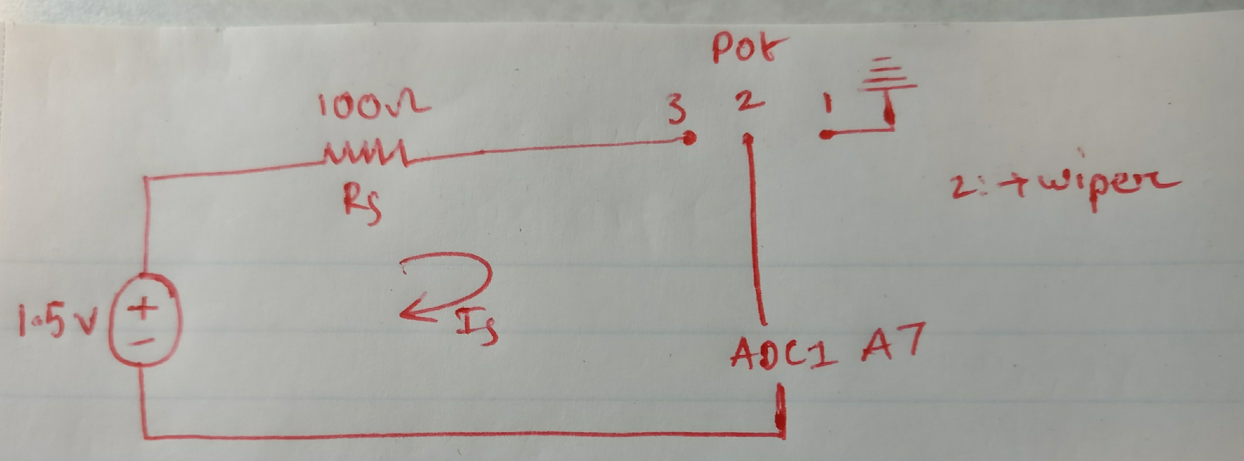
I am trying to better understand the concerto ADC module by doing a simple conversion. I am supplying a 1.5V voltage supply to the Analog Channel A7.(I am using a current limiting resistor and potentiometer before actually feeding the supply into the analog input pin, ).

What i am trying to do is verify if the ADC result register shows matches my analog voltage meter reading. So while assigning value  to the ADCCTL1.ADCREFSEL bit, what should i use? I am under the impression that i have to use the external reference voltage. And can i use the ePWM to trigger the SOC for this channel?? What other things do i keep in mind while writing the code for this?

Thank you,

Srini

  • Srini,

    I recommend that you read through the Analog Subsystem chapter of the Reference Manual for background information.

    Before programming your own application from the ground-up, I recommend that you try some of the examples from controlSUITE first. The adc_soc example would be appropriate for what you are describing: \controlSUITE\device_support\f28m36x\v220\F28M36x_examples_Control\adc_soc

    For an abridged overview of the device architecture, you can see the materials from this One-Day F28M35x Workshop.

    -Tommy

  • Thank s for your time, Tommy. I read the analog subsystems chapter. my doubts actually arise after reading page 904 where they specify the Internal/External Voltage selection and i am not sure which one is more akin to my needs. I have simulated TI examples and they use Internal bandgap and use ePWM to trigger their SOC. I Was going to follow that but i wasn't sure if i should use the internal or external reference voltage. my gut feeling is external reference. what are your thoughts??

    Thanks again,
    Srini
  • Srini,

    The choice is entirely up to you based on your design requirements.

    The internal reference is the easiest option with a full scale range (FSR) of 0V to 3.3V. Go ahead and use this if your application does not need more than 12b of precision within a 0V-3.3V FSR.

    If you require higher precision by reducing the FSR, then you can supply your own external reference voltages. Just make sure that the VREFHI/VREFLO voltages satisfy the datasheet specifications.

    -Tommy
  • Will do, Thanks a lot tommy !!
  • Hey tommy,

    I used the ADC_SOC control suite example as a framework and added my code to it. I am setting Channel ADC1A7 as SOC2 and providing EPWM1 as the trigger and setting ACQPS bit to 6. When i pass an input of 1.35 volts in the ADC Channel A7 , it's reading in the ADCResult 2 register is close to 3.02V?? Below is my Code.. am i doing something wrong?? Also changing the potentiometer setting has no effect on the ADC result value..

    EALLOW;
    GpioG1CtrlRegs.GPADIR.bit.GPIO0 = 1; //Set as output
    GpioG1CtrlRegs.GPADIR.bit.GPIO8 = 1; //Set as output
    GpioG1CtrlRegs.GPAMUX1.bit.GPIO0 = 1; //Set mux to EPWM1A
    GpioG1CtrlRegs.GPAMUX1.bit.GPIO8 = 3; //Set mux to ADCSOCAn
    EDIS;

    // Step 3. Clear all interrupts and initialize PIE vector table:
    // Disable CPU interrupts
    DINT;

    // Initialize the PIE control registers to their default state.
    // The default state is all PIE interrupts disabled and flags
    // are cleared.
    // This function is found in the F28M36x_PieCtrl.c file.
    InitPieCtrl();

    // Disable CPU interrupts and clear all CPU interrupt flags:
    IER = 0x0000;
    IFR = 0x0000;

    // Initialize the PIE vector table with pointers to the shell Interrupt
    // Service Routines (ISR).
    // This will populate the entire table, even if the interrupt
    // is not used in this example. This is useful for debug purposes.
    // The shell ISR routines are found in F28M36x_DefaultIsr.c.
    // This function is found in F28M36x_PieVect.c.
    InitPieVectTable();

    // Interrupts that are used in this example are re-mapped to
    // ISR functions found within this file.
    EALLOW; // This is needed to write to EALLOW protected register
    PieVectTable.ADCINT1 = &adc1_isr;
    EDIS; // This is needed to disable write to EALLOW protected registers

    // Step 4. Initialize all the Device Peripherals:
    // This function is found in F28M36x_InitPeripherals.c
    // InitPeripherals(); // Not required for this example
    InitAdc1(); // For this example, init the ADC

    // Step 5. User specific code, enable interrupts:

    // Enable ADCINT1 in PIE
    PieCtrlRegs.PIEIER1.bit.INTx1 = 1; // Enable INT 1.1 in the PIE
    IER |= M_INT1; // Enable CPU Interrupt 1
    EINT; // Enable Global interrupt INTM
    ERTM; // Enable Global realtime interrupt DBGM

    LoopCount = 0;
    ConversionCount = 0;

    // Configure ADC
    EALLOW;
    Adc1Regs.ADCCTL2.bit.ADCNONOVERLAP = 1; // Enable non-overlap mode i.e.
    // conversion and future
    // sampling events don't overlap
    Adc1Regs.ADCCTL1.bit.INTPULSEPOS = 1; // ADCINT1 trips after
    // AdcResults latch
    Adc1Regs.INTSEL1N2.bit.INT1E = 1; // Enabled ADCINT1
    Adc1Regs.INTSEL1N2.bit.INT1CONT = 0; // Disable ADCINT1 Continuous
    // mode
    Adc1Regs.INTSEL1N2.bit.INT1SEL = 0; // setup EOC0 to trigger ADCINT1
    // to fire
    Adc1Regs.ADCSOC0CTL.bit.CHSEL = 0; // set SOC0 channel select to
    // ADC1A0
    Adc1Regs.ADCSOC1CTL.bit.CHSEL = 2; // set SOC1 channel select to
    // ADC1A2
    Adc1Regs.ADCSOC2CTL.bit.CHSEL = 7; // set SOC2 channel to ADC1A7

    AnalogSysctrlRegs.TRIG1SEL.all = 5; // Assigning EPWM1SOCA to
    // ADC TRIGGER 1 of the ADC module

    Adc1Regs.ADCSOC0CTL.bit.TRIGSEL = 5; // Set SOC0 start trigger to
    // ADC Trigger 1(EPWM1 SOCA) of the
    // adc
    Adc1Regs.ADCSOC1CTL.bit.TRIGSEL = 5; // set SOC1 start trigger to
    // ADC Trigger 1(EPWM1 SOCA) of the
    // adc
    Adc1Regs.ADCSOC2CTL.bit.TRIGSEL = 5; // set SOC2 start trigger to
    // ADC Trigger 1(EPWM1 SOCA) of the
    // adc

    Adc1Regs.ADCSOC0CTL.bit.ACQPS = 6; // set SOC0 S/H Window to 7 ADC
    // Clock Cycles, (6 ACQPS plus
    // 1)
    Adc1Regs.ADCSOC1CTL.bit.ACQPS = 6; // set SOC1 S/H Window to 7 ADC
    // Clock Cycles, (6 ACQPS plus
    // 1)
    Adc1Regs.ADCSOC1CTL.bit.ACQPS = 6; // set SOC1 S/H Window to 7 ADC
    // Clock Cycles, (6 ACQPS plus
    // 1)

    EDIS;

    //// Assumes ePWM1 clock is already enabled in InitSysCtrl();

    //Set event triggers (SOCA) for ADC SOC1
    EPwm1Regs.ETSEL.bit.SOCAEN = 1; // Enable SOC on A group
    EPwm1Regs.ETSEL.bit.SOCASEL = ET_CTRU_CMPA; // Select SOC from CMPA on
    // upcount
    EPwm1Regs.ETPS.bit.SOCAPRD = 3; // Generate pulse on every 3rd
    // event

    // Time-base registers
    EPwm1Regs.TBPRD = PERIOD; // Set timer period, PWM
    // frequency = 1 / period
    EPwm1Regs.TBPHS.all = 0; // Time-Base Phase Register
    EPwm1Regs.TBCTR = 0; // Time-Base Counter Register
    EPwm1Regs.TBCTL.bit.PRDLD = TB_IMMEDIATE; // Set Immediate load
    EPwm1Regs.TBCTL.bit.CTRMODE = TB_COUNT_UP; // Count-up mode: used for
    // asymmetric PWM
    EPwm1Regs.TBCTL.bit.PHSEN = TB_DISABLE; // Disable phase loading
    EPwm1Regs.TBCTL.bit.SYNCOSEL = TB_SYNC_DISABLE;
    EPwm1Regs.TBCTL.bit.HSPCLKDIV = TB_DIV1;
    EPwm1Regs.TBCTL.bit.CLKDIV = TB_DIV1;

    // Setup shadow register load on ZERO

    EPwm1Regs.CMPCTL.bit.SHDWAMODE = CC_SHADOW;
    EPwm1Regs.CMPCTL.bit.SHDWBMODE = CC_SHADOW;
    EPwm1Regs.CMPCTL.bit.LOADAMODE = CC_CTR_ZERO; // load on CTR=Zero
    EPwm1Regs.CMPCTL.bit.LOADBMODE = CC_CTR_ZERO; // load on CTR=Zero

    // Set Compare values

    EPwm1Regs.CMPA.half.CMPA = DUTY_CYCLE_A; // Set duty 50% initially
    EPwm1Regs.CMPB = DUTY_CYCLE_B; // Set duty 50% initially

    // Set actions

    EPwm1Regs.AQCTLA.bit.ZRO = AQ_SET; // Set PWM2A on Zero
    EPwm1Regs.AQCTLA.bit.CAU = AQ_CLEAR; // Clear PWM2A on event A, up
    // count

    EPwm1Regs.AQCTLB.bit.ZRO = AQ_CLEAR; // Set PWM2B on Zero
    EPwm1Regs.AQCTLB.bit.CBU = AQ_SET; // Clear PWM2B on event B, up
    // count

    // Wait for ADC interrupt
    for(;;)
    {
    LoopCount++;
    }
    }

    __interrupt void adc1_isr(void)
    {
    Voltage1[ConversionCount] = Adc1Result.ADCRESULT0;
    Voltage2[ConversionCount] = Adc1Result.ADCRESULT1;
    Voltage3[ConversionCount] = Adc1Result.ADCRESULT2;

    // If 20 conversions have been logged, start over
    if(ConversionCount == 9)
    {
    ConversionCount = 0;
    }
    else ConversionCount++;

    Adc1Regs.ADCINTFLGCLR.bit.ADCINT1 = 1; //Clear ADCINT1 flag reinitialize
    // for next SOC
    PieCtrlRegs.PIEACK.all = PIEACK_GROUP1; // Acknowledge interrupt to PIE

    return;
    }
  • Srini,

    It looks like you are configuring the SOC1 ACQPS setting twice instead of the SOC2 ACQPS.

    -Tommy
  • Yes, i noticed it and changed that but i am still not getting a right voltage reading.
    My supply is rated at 1.5V.
    The input from the potentiometer into the Analog pin as 1.368 V.

    So for that voltage reading i should get a result of 1698 approx in my ADC RESULT 2 register. But i end up getting 3753. which translates to 3.024V. Any idea what i could be missing here??
  • It could be that your resistors are slowing down the charging (or discharging) of the ADC hold capacitor while sampling A7.  You can confirm this by looking at A7 with an oscilloscope during the ADC conversion to see if there is voltage disturbance at the pin.

    If this is the case, you can experiment with a combination of the following to improve the conversion:

    • Increase ACQPS
    • Reduce series resistance (can go down to 0)
    • If it's a low-bandwidth signal, add a large capacitor (nF to uF range) between the resistor and A7

    -Tommy

  • Thank you, will check the scope and look for any disturbance.

  • Hey tommy,

    I looked at the scope measurement for the analog input on A7 and there is no voltage disturbance on that pin. I get a constant DC pulse of 1.4 V at 100 percent pot setting. Nevertheless i tried some of your suggestions to see what happens and i am at max ACQPS value, chose a Rs value of 10 ohms and it actually didn't have much of an impact on the analog readings. They are still disproportionate. Adding the capacitor effected the input voltae in the sense that it never went to 0. stays between 1.2V and 1.4V. (maybe because i don't have a low bandwidth).

    Currently this is what i have,
    A 1.5 volt input trough a 100 ohm resistor and a 1K Pot into ADC1A7 channel. The Analog input measured using a multimeter on this channel is 1.369 V at 100 % pot setting and 0V at 0% pot setting. The scope output looks a perfect DC signal of 1.4 V and 0V respectively.

    But for these two pot settings i am getting a Analog reading of 3566 and 1862 respectively. This translates to a voltage reading of 2.873V in the 100% pot setting and 1.50 V in the 0% pot setting. There is a linear decrease on the voltage reading as i reduce the pot setting. I graphed it and the slope is nearly identical at different instants. Do you think this may be an offset error?? or do you have any other suggestion. Appreciate your time and assistance. Kindly let me know what you think.

    Thank you,
    Srini
  • Srini,

    Can you show a schematic of how you have connected everything? Do the other ADC channels have the same behavior?

    The potentiometer will contribute to Rs so you can also apply the 1.5V input directly to A7. You can also try to sample the VDD12 or VDD18 supplies directly in case there is poor grounding between your external voltage and the device.

    -Tommy
  • This is the circuit connection. I am not using the docking board provided by TI. Using a personalized board where i have connectors for the ADC Channels.

    The other ADC Channels used in the code are from the TI Example. Those registers have a value in the 3800 range approx.

    I removed the Rs and i am only using the potentiometer and there is still no change to the analog reading.

  • Srini,

    Can you confirm that the 1.5V ground is connected to both the Pot-1 terminal and VSSA on your board?

    Your drawing shows A7 to be connected to both the 1.5V ground and Pot-2?

    -Tommy
  • Sorry tommy. I think that circuit drawing is a bit misleading. Below is the schematic

    In the above picture,

    VREF BUFFEXT is a 1.5V signal. R6 is Rs and is equal to 100 ohms. P1 is the 1k Potentiometer. one end of it is grounded and the wiper feeds the input to AD2B6.. but instead of using ADC2B6 i am using ADC1A7.

    the only ground connection in the schematic is from the pot.

  • This is the ADC Channel connector

    Essential the node for ADC1A7 is in the second pin of this connector. The wiper of the pot feeds a 1.38 V signal to it. The ground of the wiper is connected to one of the ground pins in this connector( pin 11 to be accurate).

  • Can you confirm that the ground reference for VREF BUFFEXT is connected to VSSA as well?
  • Yes, it is connected.
  • I figured it out tommy. Thanks for all the help.