This thread has been locked.

If you have a related question, please click the "Ask a related question" button in the top right corner. The newly created question will be automatically linked to this question.

CCS/LAUNCHXL-F28379D: questions & problem for ADC part in TMS320F28379D

Part Number: LAUNCHXL-F28379D
Other Parts Discussed in Thread: OPA350

Tool/software: Code Composer Studio

Hi,

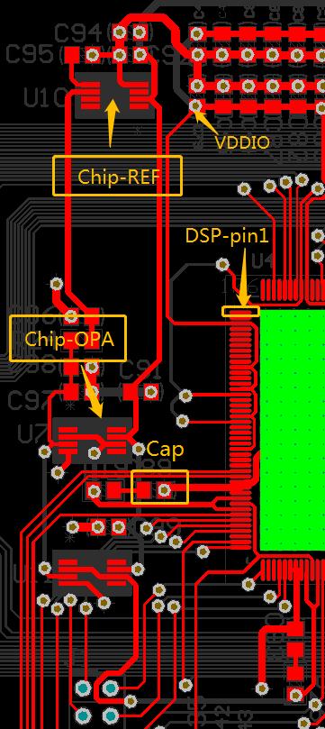
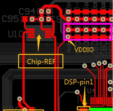
I got some questions in TMS320F38279D ADC program and hardware using differential mode(16bit).

The sinusodial signal with about 1.9V Vpp and 1KHz frequence was converted into digital signal by using the adc module in the  board LAUNCHXL-F28379D. The running result shows below. It can be seen that the waveform get phase loss in the black dotted line box. Why does it happened?

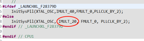
I try to make a circuit board using master chip TMS3220F28379D to realize A/D convertion. The A/D test I made using the same program. The result compared to LAUNCHXL-F28379D result is show below. It seems that it is quite a bit wrong except the Vpp.  What do I missed? 

Best regards,

DITNY.

  • Hi Yuansheng,

    It is somewhat hard to say what could have gone wrong without seeing the circuit, but you should start by looking at the following items:

    • VDD, VDDIO, and VDDA voltages are as expected and decoupling capacitors for each supply is appropriate magnitude and placement.
    • VREFHI driving circuit is appropriate and producing the desired voltage.
      • Driving op-amp is reasonably close to the device
      • Appropriatly sized capacitor is between VREFHI and VREFLO and is very close to these pins
        • Damping resistor on this capacitor is present such that op-amp will be stable (or extraction of board parasitics has been done and found to be large enough without discrete damping resistor)
      • You might want to scope the output of this circuit and ensure it isn't oscillating.  
    • VREFLO makes a strong connection to VSSA
    • VSSA is connected to the digital ground VSS
      • (Either these are the same net, or the two planes are joined at a single point near/under the device)
    • ADC input conditioning circuits are powered and operating as desired
    • ADC input common mode is within 50mV of VREFHI/2

  • Sorry, missed a couple:

    • X1 input frequency is as desired
    • After initializations are run, PLL settings appear correct in the expressions window
    • Enable XCLKOUT and ensure that SYSCLK is as desired (probably 200MHz)
    • After initializations, ADC PRESCALE is set as desired (probably the value should be '6')
    • ADC ACQPS for the SOC in question is set appropriately (probably at least ACQPS = 63 => S+H of 320ns)
    • Input is hooked up to both ADCp and ADCn channels and these channels correspond to the value read-back from CHSEL from the SOC in question 

  • Hi, Devin Cottier.

    Thanks for your reply!

    I've test the voltage inputs like VDD, VDDIO, VDDA and VREFHI and their voltage is as desired. I think the ADC input circuit and the DSP program may be ok because they all works in LaunchXL-F28379D pad  which my board imitates in the ADC module part.

    The schematic diagram and PCB pictures of ADC module part is shown below.

    And what does it mean by 'You might want to scope the output of this circuit and ensure it isn't oscillating.'? In other way, how can I test it?

    Best regards, DITNY.

  • Hi DITNY,

    Are these the decoupling capacitors for the VDDIO rail?

    These are to absorb high frequency transients from the power supply and as such need to be physically distributed to each supply pin and be close to the device.  This is probably not causing the issue you are observing, but this will certainly impact the noise and reliability of your design. 

    The concern with the reference oscillating is that op-amps are not good at driving capacitive loads.  With a large capacitive load, the op-amp output can oscillate.  You'd wan to scope the VREFHI pin during ADC operation to look for noticeable ringing.  If you are using the launchpad design of OPA350 + 0.1ohm + 22uF we have simulated the circuit to ensure it is stable;  this should be OK as long as you don't add significant additional capacitance to the pin.  

    You also might want capacitors on the ADC inputs.  About 220pF to 330pF, COF or NPO type.  Single-ended inputs have the capacitor between input and ground, differential inputs have the capacitor between the two pins (on the launchpad these caps would go on the boosterpack boards).

    Are you sure the input signal is making it to the input pins undistorted?

  • Hi,Devin Cottier.

    I deleted several program statements in ADC interrupt whose trigger source is EPWM. When running the program,  it can roughly show the  waveform of  input signal. But the wave frequence seems to be not right in ADCAdcaResults value. The input signal is 1KHz, and it should have about 10 points per period. But u can see in the picture that it just have 6 pionts per period as shown below.(The TBPRD I set is 0x1000,  and CHSPCLKDIV and CLKDIV is default). How does it happen? Or do I miss something?

  • Hi DITNY,

    0x1000 = 4096.

    Is the ePWM in up-count mode or up-down mode?

    It is probably worthwhile to list out all the clock settings like:
    X1 input
    PLL multiplier
    PLL divider
    Resulting SYSCLK from PLL ouput
    ePWM dividers

    And then verify what you can. e.g. SYSYCLK you can verify using the XCLKOUT functionality, PLL multiplier you can verify by looking at the ClkCfgRegs in the expressions window
  • Hi,Devin Cottier.

    The ePWM is in up-count. The X1 input is a 10MHz crystal.

    What I use to debug is device support exmaple code of TI , 'adc_soc_epwm_cpu01'. And I do not changge the code in the settings you mentioned.
    As I see, the setting is :IMULT_40,FMULT_0,PLLCLK_BY_2. So the PLL multiplier=40, PLL divider=1, right?
    And can you tell me where to find the settings of:
    Resulting SYSCLK from PLL ouput
    ePWM dividers?

    Best regards,DITNY.
  • Hi DITYNY,

    If the ePWM clock is 100MHz, the ePWM is in up-count mode, and the period is 4096 counts then the sample rate should be about 24kHz. It looks like you are two orders of magnitude off of that (6kHz).

    Check the ePMW multiplier in the expressions window to see if it is 20 or 40...you may not have the flag defined that tells the code this is a launchpad?

    Check the other ePWM dividers. You should only need one /2 divider to get to 100MHz from 200MHz SYSCCLK.

    You may also want to verify the SYSCLK using XCLKOUT.

    You can also setup the ePWM to toggle a pin at the same time the trigger occurs so that you can experimentally verify the sample rate.
  • Hi,Devin Cottier.

    You are right. As you said, I think I did not  have the flag defined that tells the code this is a launchpad. Because I change the IMULT into 40 and it works in device support exmaple code of TI for Launchpad and self-made board,  which have about 12 points per period.

    But there raises another question. When change the IMULT into 40, the code ,which imitates device support exmaple code of TI , works in lauchpad but not in my board.  The results in my self-made board is similar to the result when I first proposed  this post.  

    The chip I used is 28379DPTPS and in lauchpad is 28379DZWTT. Is that happens connected with chips different?

    And can you tell me how to have the flag defined that tells the code this is a launchpad?  

    Best regards,

    DITNY.

  • Hi DITNY,

    For defining the symbol, see .

    There shouldn't be anything different between the two devices you listed w.r.t. PLL frequency, ADC triggering frequency, ADC conversion time, etc.