This thread has been locked.

If you have a related question, please click the "Ask a related question" button in the top right corner. The newly created question will be automatically linked to this question.

The output of gpio under different loads.

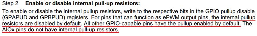
As the "TMS320x2803x Piccolo System Control and Interrupts Reference Guide" says:

For example, the following two gpios:

I tried a test like this:

The program is simple:

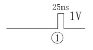
Remove the R1 R2,the measurement results using oscilloscope are as follows:

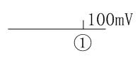
Because of the default setting of pull up resistors, they are right!

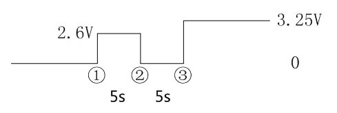
If I keep the R1 R2, the measurement results are as follows:

Then I changed R2 different resistors:

Pin

①(V)

②(V)

③(V)

R2(Ω)

GPIO22

3.25

0

3.25

NO

0.086

0.008

3.03

660

0.043

0.008

2.85

330

0.013

0.006

2.16

100

0

0

0.46

10

As the " General Purpose IO (GPIO) FAQ for C2000" says:

The datasheet says:

So, in the stage①,I=0.086V/660Ω=130uA, 330Ω、100Ωalso like this.

But, in the stage③,when gpio output 1, what causes the voltage to fall,and the current isn't in range.

I think the current source drive ability is not enough, but the current is a few hundred mA,where does the other power come from?

How to understand the recommended operating conditions 4mA?

Thanks,LC

  • LC,

    you have these pins configured as an output correct?

    Liang Che said:
    But, in the stage③,when gpio output 1, what causes the voltage to fall,and the current isn't in range.

    You have a very strong pull down resistor, the IO buffer does not have enough drive strength to pull the pin all the way to 3.3V. 

    Liang Che said:

    I think the current source drive ability is not enough, but the current is a few hundred mA,where does the other power come from?

    How to understand the recommended operating conditions 4mA?

    The Recommended operating conditions table is a list of conditions you should not exceed, if you do the information in the datasheet will no longer be valid.

    The device 'can', BUT IT SHOULD NOT, source more than 4mA. If you supply a few hundred mAs through a pin it has been damaged. The effects may not prevent the device from functioning but some damage has occurred. If you continue to source or sink too much current the IO buffer will stop working.

    Regards,
    Cody 

  • Hi Cody,

    Thanks for your answer. 

    If I want to control a photo-mos relay,could it be achieved without another transistor or MOS?

    The photo-mos relay is AQY225R1SX from Panasonic,the LED turn on current is 0.5-3mA,the LED continuous operating current is 5-30mA.

    But DSP source or sink current is 4mA(Other some 8mA pins are not considered).It is possible the photo-mos relay can continuous operating with 4mA,but at the critical condition,what is your opinion?

    Besides,should I use high level or low level to drive? Because I don't want photo-mos relay open at stage①.I tried a test like this:

    1.low level drive

    GPIO2(default no pull up)

    GPIO22(default pull up)

    Maybe photo-mos relay's LED already on,the voltage drop is generated,but GPIO22 internal current source works.

    2.high level drive

    GPIO2(default no pull up)

    GPIO22(default pull up)

    The photo-mos relay's turn on time is 0.25ms.

    Do you think GPIO2(default no pull up)with high level drive is better?

    Regards,
    LC

  • LC,

    you will need to use an LED driver if the current exceeds 4mA.

    As a general rule its better to sink current rather than source current, so "1.low drive level" is more common. You'll have to determine which  method is better for the behavior you want.


    Regards,
    Cody