This thread has been locked.

If you have a related question, please click the "Ask a related question" button in the top right corner. The newly created question will be automatically linked to this question.

LAUNCHXL-F28069M: ILI9341 and 4wire SPI

Part Number: LAUNCHXL-F28069M

Hi,

I have the following ili9341 lcd

The display is connected as described:

/**
 * ILI9341 <--> LAUNCHXL-F28069M interconnect
 * ILI9341		LAUNCHXL-F28069M				InitSpiaGpio
 * -------------------------------------------------------------
 * SDO(MISO)	J2(14)	1SPI_SO		(GPIO17)	(SPISOMIA)
 * LED			J4(34)	GPIO		(GPIO13)
 * SCK			J1(7)	1SPI_CLK	(GPIO18)	(SPICLKA)
 * SDI(MOSI)	J2(15)	1SPI_SI		(GPIO16)	(SPISIMOA)
 * DC			J2(18)	GPIO		(GPIO44)
 * RESET		J1(8)	GPIO		(GPIO22)
 * CS			J2(19)	1SPI_CS		(GPIO19)	(SPISTEA)
 * GND
 * VCC
 */

I have the following code to drive the LCD:

void init_spi_ili9341(void)
{
	EALLOW;

	/**
	 * Enable internal pull-up for the selected pins
	 * Pull-ups can be enabled or disabled by the user.
	 * This will enable the pullups for the specified pins.
	 */
	GpioCtrlRegs.GPAPUD.bit.GPIO16 = 0;		/* pull-up on GPIO16 (SPISIMOA)		*/
	GpioCtrlRegs.GPAPUD.bit.GPIO17 = 0;		/* pull-up on GPIO17 (SPISOMIA)		*/
	GpioCtrlRegs.GPAPUD.bit.GPIO18 = 0;		/* pull-up on GPIO18 (SPICLKA)		*/
	GpioCtrlRegs.GPAPUD.bit.GPIO19 = 0;		/* pull-up on GPIO19 (SPISTEA)		*/

	/**
	 * Set qualification for selected pins to asynch only
	 * This will select asynch (no qualification) for the selected pins.
	 */
	GpioCtrlRegs.GPAQSEL2.bit.GPIO16 = 3;	/* Asynch input GPIO16 (SPISIMOA)	*/
	GpioCtrlRegs.GPAQSEL2.bit.GPIO17 = 3;	/* Asynch input GPIO17 (SPISOMIA)	*/
	GpioCtrlRegs.GPAQSEL2.bit.GPIO18 = 3;	/* Asynch input GPIO18 (SPICLKA)	*/
	GpioCtrlRegs.GPAQSEL2.bit.GPIO19 = 3;	/* Asynch input GPIO19 (SPISTEA)	*/

	/**
	 * Configure SPI-A pins using GPIO regs
	 * This specifies which of the possible GPIO pins will be SPI functional
	 * pins.
	 */
	GpioCtrlRegs.GPAMUX2.bit.GPIO16 = 1;	/* Configure GPIO16 as SPISIMOA		*/
	GpioCtrlRegs.GPAMUX2.bit.GPIO17 = 1;	/* Configure GPIO17 as SPISOMIA		*/
	GpioCtrlRegs.GPAMUX2.bit.GPIO18 = 1;	/* Configure GPIO18 as SPICLKA		*/
	GpioCtrlRegs.GPAMUX2.bit.GPIO19 = 1;	/* Configure GPIO19 as SPISTEA		*/

	EDIS;
}

void init_spi(void)
{
	SpiaRegs.SPICCR.bit.SPISWRESET = 0;		/* Reset SPI						*/

	SpiaRegs.SPIPRI.bit.TRIWIRE = 0;		/* SPI 4 wire MODE enabled			*/
	SpiaRegs.SPICCR.bit.SPICHAR = 0x7;		/* 8 bits							*/
	SpiaRegs.SPICCR.bit.CLKPOLARITY = 0;	/* CPOL = 0							*/
	SpiaRegs.SPICTL.bit.MASTER_SLAVE = 1;	/* Master							*/
	SpiaRegs.SPICTL.bit.CLK_PHASE = 0;		/* CPHA = 0, normal mode			*/
	SpiaRegs.SPICTL.bit.TALK = 1;			/* enable transmission				*/
	SpiaRegs.SPISTS.all = 0x0000;			/* clear status flags				*/
	SpiaRegs.SPIBRR = 0x0063;				/* Baud Rate						*/
	SpiaRegs.SPIFFTX.bit.SPIFFENA = 1;		/* FIFO enhancement enabled 		*/
	SpiaRegs.SPIFFTX.bit.SPIRST = 1;		/* FIFO can resume Rx/Tx			*/
	SpiaRegs.SPIFFCT.all = 0x00;			/* no delays						*/
	SpiaRegs.SPIPRI.bit.FREE = 1;			/* Free run							*/

	SpiaRegs.SPICCR.bit.SPISWRESET = 1;		/* Enable SPI						*/
	SpiaRegs.SPIFFTX.bit.TXFIFO = 1;		/* Re enable TX FIFO				*/
	SpiaRegs.SPIFFRX.bit.RXFIFORESET = 1;	/* Re enable RX FIFO				*/
}

/**
 * ILI9341 <--> LAUNCHXL-F28069M interconnect
 * ILI9341		LAUNCHXL-F28069M				InitSpiaGpio
 * -------------------------------------------------------------
 * SDO(MISO)	J2(14)	1SPI_SO		(GPIO17)	(SPISOMIA)
 * LED			J4(34)	GPIO		(GPIO13)
 * SCK			J1(7)	1SPI_CLK	(GPIO18)	(SPICLKA)
 * SDI(MOSI)	J2(15)	1SPI_SI		(GPIO16)	(SPISIMOA)
 * DC			J2(18)	GPIO		(GPIO44)
 * RESET		J1(8)	GPIO		(GPIO22)
 * CS			J2(19)	1SPI_CS		(GPIO19)	(SPISTEA)
 * GND
 * VCC
 */

int spi_wr(Uint8 data)
{
	Uint16 rd, tmp = data << 8;

	SpiaRegs.SPITXBUF = tmp;				/* master TX data			*/
	while (SpiaRegs.SPIFFRX.bit.RXFFST != 1);	/* wait for data Rx		*/
	rd = SpiaRegs.SPIRXBUF;					/* Read Rx data				*/
	if (rd != tmp)
		return -1;
	return 0;
}

int spi_wr16(Uint16 data)
{
	Uint16 rd, tmp;

	tmp = (data >> 8) << 8;					/* MSB first, left aligned	*/
	SpiaRegs.SPITXBUF = tmp;
	while (SpiaRegs.SPIFFRX.bit.RXFFST != 1);
	rd = SpiaRegs.SPIRXBUF;
	if (rd != tmp)
		return -1;

	tmp = (data & 0xff) << 8;				/* LSB next, left aligned	*/
	SpiaRegs.SPITXBUF = tmp;
	while (SpiaRegs.SPIFFRX.bit.RXFFST != 1);
	rd = SpiaRegs.SPIRXBUF;
	if (rd != tmp)
		return -1;

	return 0;
}

void lcd_cmd(Uint8 cmd)
{
	/**
	 * D/CX bit is “low”, the transmission byte is interpreted
	 * as a command byte.
	 */
	GpioDataRegs.GPBCLEAR.bit.GPIO44 = 1;	/* pull down D/C pin		*/
	spi_wr(cmd);
	GpioDataRegs.GPBSET.bit.GPIO44 = 1;		/* pull up D/C pin			*/
}

void lcd_dat(Uint8 *data, Uint32 len)
{
	Uint32 i;

	for (i = 0; i < len; i++)
		spi_wr(data[i]);
}

void lcd_pixels(Uint16 color, Uint32 count)
{
	Uint16 i;

	for (i = 0; i < count; i++)
		spi_wr16(color);
}

const Uint8 ili9341_init[] = {
        // Power control A
        6, LCD_POWERA, 0x39, 0x2C, 0x00, 0x34, 0x02,
        // Power control B
        4, LCD_POWERB, 0x00, 0xC1, 0x30,
        // Driver timing control A
        4, LCD_DTCA, 0x85, 0x00, 0x78,
        // Driver timing control B
        3, LCD_DTCB, 0x00, 0x00,
        // Power on sequence control
        5, LCD_POWER_SEQ, 0x64, 0x03, 0x12, 0x81,
        // Pump ratio control
        2, LCD_PRC, 0x20,
        // Power control 1
        2, LCD_POWER1, 0x23,
        // Power control 2
        2, LCD_POWER2, 0x10,
        // VCOM control 1
        3, LCD_VCOM1, 0x3E, 0x28,
        // VCOM cotnrol 2
        2, LCD_VCOM2, 0x86,
        // Memory access control
        2, LCD_MAC, 0x48,
        // Pixel format set
        2, LCD_PIXEL_FORMAT, 0x55,
        // Frame rate control
        3, LCD_FRMCTR1, 0x00, 0x18,
        // Display function control
        4, LCD_DFC, 0x08, 0x82, 0x27,
        // 3Gamma function disable
        2, LCD_3GAMMA_EN, 0x00,

		// Column Address
		5, LCD_COLUMN_ADDR, 0x00, 0x00, 0x00, 0xEF,
		// Page Address
		5, LCD_PAGE_ADDR, 0x00, 0x00, 0x01, 0x3F,

        // Gamma curve selected
        2, LCD_GAMMA, 0x01,
        // Set positive gamma
        16, LCD_PGAMMA, 0x0F, 0x29, 0x24, 0x0C, 0x0E, 0x09, 0x4E, 0x78, 0x3c, 0x09, 0x13, 0x05, 0x17, 0x11, 0x00,
        16, LCD_NGAMMA, 0x00, 0x16, 0x1b, 0x04, 0x11, 0x07, 0x31, 0x33, 0x42, 0x05, 0x0c, 0x0a, 0x28, 0x2f, 0x0F,
        0
};

void lcd_init(void)
{
	Uint8 count;
	Uint8 *address = (Uint8 *) ili9341_init;

	while (1) {
		count = *(address++);
		if (count-- == 0)
			break;

		lcd_cmd(*(address++));
		lcd_dat(address, count);
		address += count;
	}
}

void lcd_reset(void)
{
	GpioDataRegs.GPACLEAR.bit.GPIO22 = 1;	/* RESET = 0				*/
	DELAY_US(10000);						/* wait 10ms				*/
	GpioDataRegs.GPASET.bit.GPIO22 = 1;		/* RESET = 1				*/
	DELAY_US(50000);						/* wait 50mS				*/
}

void lcd_standby(void)
{
	lcd_cmd(LCD_SLEEP_OUT);					/* 0x11						*/
	DELAY_US(150000);						/* Wait 150mS				*/
	lcd_cmd(LCD_DISPLAY_ON);				/* 0x29						*/
}

void lcd_orientation(Uint8 pos)
{
	lcd_cmd(LCD_MAC);
	lcd_dat(&pos, 1);
}

static void lcd_set_window(Uint16 x1, Uint16 y1, Uint16 x2, Uint16 y2)
{
	lcd_cmd(LCD_COLUMN_ADDR);				/* 0x2a						*/
	spi_wr16(x1);							/* Start Column				*/
	spi_wr16(x2);							/* End Column				*/

	lcd_cmd(LCD_PAGE_ADDR);					/* 0x2b						*/
	spi_wr16(y1);							/* Start Page				*/
	spi_wr16(y2);							/* End Page					*/
}

// width = 0, is 1 pixel wide
// height = 0, is 1 pixel high
void lcd_window_fill(Uint16 x_start,
		     	 	 Uint16 y_start,
					 Uint16 width,
					 Uint16 height,
					 Uint16 color)
{
	Uint32 pixels = width * height;

	lcd_set_window(x_start,
		       	   y_start,
				   (Uint16) (x_start + width - 1),
				   (Uint16) (y_start + height - 1));

	lcd_cmd(LCD_GRAM);						/* 0x2c						*/
	lcd_pixels(color, pixels);
}

void main(void)
{
	InitSysCtrl();							/* PLL, WatchDog, Peripheral Clk's	*/
	init_spi_ili9341();						/* setup gpio for ili9341 spi		*/

	DINT;									/* Disable all CPU interrupts		*/
	IER = 0x0000;							/* Clear all CPU interrupts			*/
	IFR = 0x0000;

	InitPieCtrl();
	InitPieVectTable();

	EALLOW;
	/* disable pullups		*/
	GpioCtrlRegs.GPAPUD.bit.GPIO13 = 1;		/* disable pullup for Backlight		*/
	GpioCtrlRegs.GPAPUD.bit.GPIO22 = 1;		/* disable pullup for RESET			*/
	GpioCtrlRegs.GPBPUD.bit.GPIO44 = 1;		/* disable pullup for D/C			*/

	/* configure as GPIO	*/
	GpioCtrlRegs.GPAMUX1.bit.GPIO13 = 0;	/* GPIO::Backlight LED				*/
	GpioCtrlRegs.GPAMUX2.bit.GPIO22 = 0;	/* GPIO::RESET						*/
	GpioCtrlRegs.GPBMUX1.bit.GPIO44 = 0;	/* GPIO::D/C						*/

	/* configure as output	*/
	GpioCtrlRegs.GPADIR.bit.GPIO13 = 1;		/* Output::Backlight				*/
	GpioCtrlRegs.GPADIR.bit.GPIO22 = 1;		/* Output::Reset					*/
	GpioCtrlRegs.GPBDIR.bit.GPIO44 = 1;		/* Output::D/C						*/
	EDIS;

	/* set default states	*/
	GpioDataRegs.GPASET.bit.GPIO22 = 1;		/* RESET default HIGH (Release)		*/
	GpioDataRegs.GPBSET.bit.GPIO44 = 1;		/* D/C default HIGH (Data MODE)		*/
	GpioDataRegs.GPASET.bit.GPIO13 = 1;		/* Display Backlight ON				*/

	/* LCD RESET			*/
	lcd_reset();							/* Force LCD Hard RESET				*/
	GpioDataRegs.GPACLEAR.bit.GPIO13 = 1;	/* Enable Backlight after Init		*/

	init_spi();								/* Initialize SPI peripheral		*/

	lcd_standby();							/* Display ON, standby				*/
	lcd_init();								/* Display fully configured			*/
	lcd_orientation(LANDSCAPE);				/* Display orientation				*/

	GpioDataRegs.GPASET.bit.GPIO13 = 1;		/* Backlight::ON					*/
	lcd_window_fill(0, 0, 320, 240, 0x7e0);	/* clear screen (Green)				*/

	while (1) {}
}

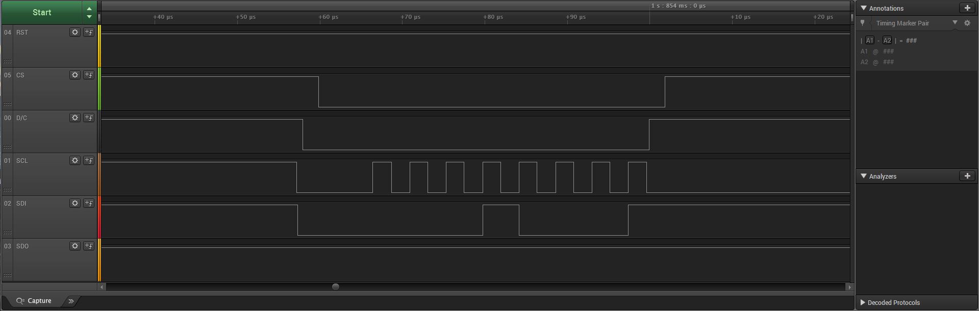
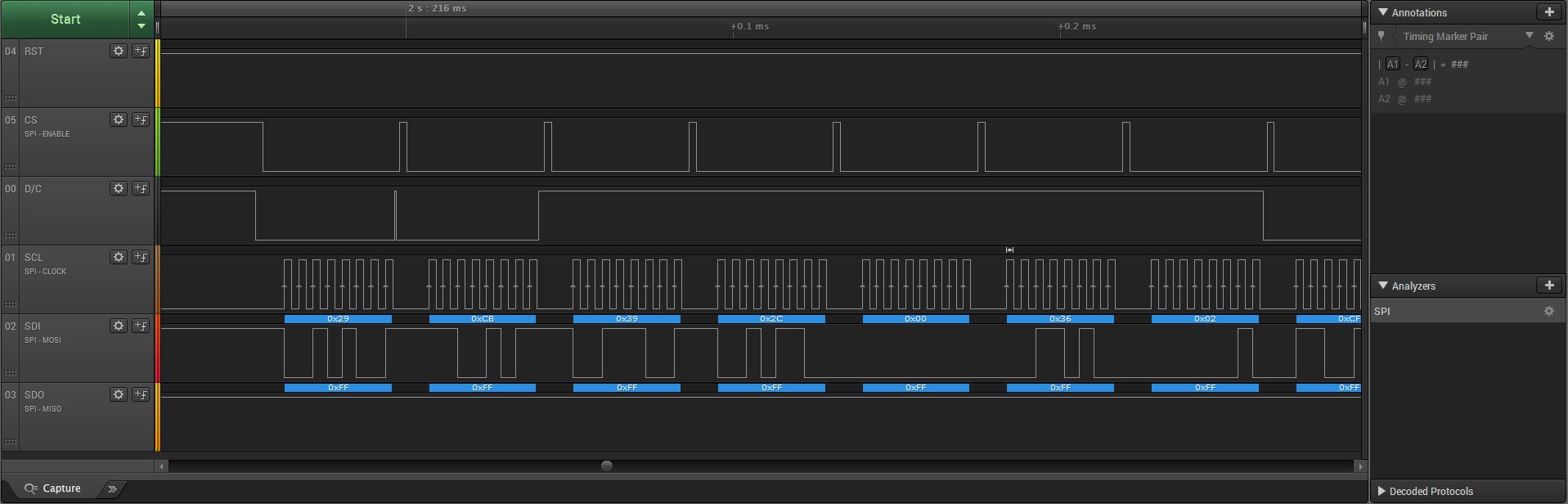
The waveforms SPI_WR looks thus:

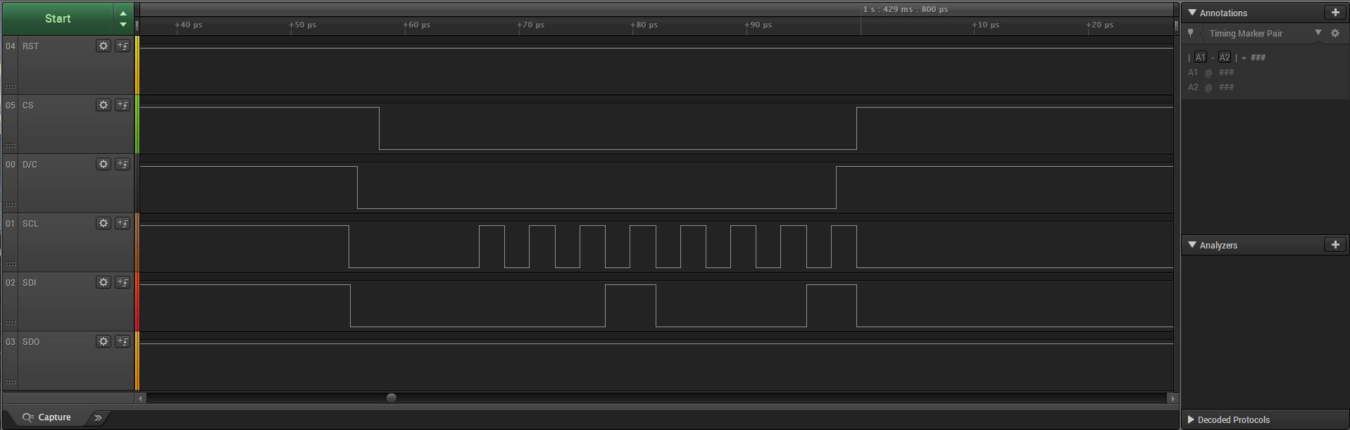
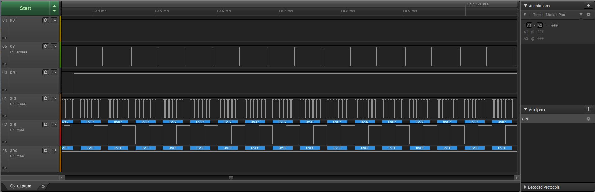
and the SPIWR16 looks thus:

I've been expecting the display to be filled with GREEN, but display seems void of anything:

The display is actually white, but the camera makes the LCD appear bluish.

Given that nothing is visible on the display that I've written to it, but when the SPI Clk Phase is changed from

    SpiaRegs.SPICTL.bit.CLK_PHASE = 0;        /* CPHA = 0, normal mode            */

to

    SpiaRegs.SPICTL.bit.CLK_PHASE = 1;        /* SPICLK delayed by one half-cycle          */

Now the display appears thus:

I wonder whether anything is wrong with my spi writes. If not, wondering what else could be wrong ? Though the window area which is filled is not as expected, the color is exactly what was expected. The LCD command/data sequence has been working exactly as expected on a STM32 Cortex M3 previously.

Also the ILI9341 SDO line should be sending the data back to the Master ? But can't see that either ?

The ILI9341 appears to use a Normal CLK Phase, but the display doesn't seem to like that; Unless there is an issue with my SPI writes.

I am slightly lost here. Can someone help, please ?

Thanks,

Manu

  • Forgot to mention the following:

    When
    SpiaRegs.SPICCR.bit.CLKPOLARITY = 0; /* CPOL = 0 */
    SpiaRegs.SPICTL.bit.CLK_PHASE = 1; /* CPHA = 1 */

    The logic analyzer fails to decode the bytes when the analyzer is set to CPOL=0, CPHA=1, but it does decodes when CPOL=0, CPHA=0

    likewise when
    SpiaRegs.SPICCR.bit.CLKPOLARITY = 0; /* CPOL = 0 */
    SpiaRegs.SPICTL.bit.CLK_PHASE = 0; /* CPHA = 0, normal mode */

    The logic analyzer fails to decode the bytes when the analyzer is set to CPOL=0, CPHA=0, but it does decodes when CPOL=0, CPHA=1

    It felt a bit weird to me that probably the CPHA bit is inverted in contrast to what's stated in the TRM ? Then a quick thought was that probably the Analyzer could be buggy, but then the ILI9341 also behaved exactly the same way as the Analyzer. Quite confused though ..
  • Update:

    Found an issue in spi_wr16(Uint16 data). The read back from the Slave is 0xff in all situations, as can be verified from the logic analyzer waveform. As a result, the second spi_wr() fails to execute. Commenting out the rd != tmp comparison check does fix temporarily spi_wr16().
    Still the SPI peripheral needs to be initialized with

    SpiaRegs.SPICTL.bit.CLK_PHASE = 1;


    Still wondering why the SPI reads are all 0xff's. The display seems to display the data what's written to it though.

    Both these issues still I cant understand why. Any thoughts ?

    Thanks,

    Manu
  • Update:

    With the following code:

    void init_spi_ili9341(void)
    {
    	EALLOW;
    
    	/**
    	 * Enable internal pull-up for the selected pins
    	 * Pull-ups can be enabled or disabled by the user.
    	 * This will enable the pullups for the specified pins.
    	 */
    	GpioCtrlRegs.GPAPUD.bit.GPIO16 = 0;		/* pull-up on GPIO16 (SPISIMOA)		*/
    	GpioCtrlRegs.GPAPUD.bit.GPIO17 = 0;		/* pull-up on GPIO17 (SPISOMIA)		*/
    	GpioCtrlRegs.GPAPUD.bit.GPIO18 = 0;		/* pull-up on GPIO18 (SPICLKA)		*/
    	GpioCtrlRegs.GPAPUD.bit.GPIO19 = 0;		/* pull-up on GPIO19 (SPISTEA)		*/
    
    	/**
    	 * Set qualification for selected pins to asynch only
    	 * This will select asynch (no qualification) for the selected pins.
    	 */
    	GpioCtrlRegs.GPAQSEL2.bit.GPIO16 = 3;	/* Asynch input GPIO16 (SPISIMOA)	*/
    	GpioCtrlRegs.GPAQSEL2.bit.GPIO17 = 3;	/* Asynch input GPIO17 (SPISOMIA)	*/
    	GpioCtrlRegs.GPAQSEL2.bit.GPIO18 = 3;	/* Asynch input GPIO18 (SPICLKA)	*/
    	GpioCtrlRegs.GPAQSEL2.bit.GPIO19 = 3;	/* Asynch input GPIO19 (SPISTEA)	*/
    
    	/**
    	 * Configure SPI-A pins using GPIO regs
    	 * This specifies which of the possible GPIO pins will be SPI functional
    	 * pins.
    	 */
    	GpioCtrlRegs.GPAMUX2.bit.GPIO16 = 1;	/* Configure GPIO16 as SPISIMOA		*/
    	GpioCtrlRegs.GPAMUX2.bit.GPIO17 = 1;	/* Configure GPIO17 as SPISOMIA		*/
    	GpioCtrlRegs.GPAMUX2.bit.GPIO18 = 1;	/* Configure GPIO18 as SPICLKA		*/
    	GpioCtrlRegs.GPAMUX2.bit.GPIO19 = 1;	/* Configure GPIO19 as SPISTEA		*/
    
    	EDIS;
    }
    
    void init_spi(void)
    {
    	SpiaRegs.SPICCR.bit.SPISWRESET = 0;		/* Reset SPI						*/
    
    	SpiaRegs.SPIPRI.bit.TRIWIRE = 0;		/* SPI 4 wire MODE enabled			*/
    	SpiaRegs.SPICCR.bit.SPICHAR = 0x7;		/* 8 bits							*/
    	SpiaRegs.SPICCR.bit.CLKPOLARITY = 0;	/* CPOL = 0							*/
    	SpiaRegs.SPICTL.bit.MASTER_SLAVE = 1;	/* Master							*/
    	SpiaRegs.SPICTL.bit.CLK_PHASE = 0;		/* CPHA = 0, normal mode			*/
    	SpiaRegs.SPICTL.bit.TALK = 1;			/* enable transmission				*/
    	SpiaRegs.SPISTS.all = 0x0000;			/* clear status flags				*/
    	SpiaRegs.SPIBRR = 0x0063;				/* Baud Rate						*/
    	SpiaRegs.SPIFFTX.bit.SPIFFENA = 1;		/* FIFO enhancement enabled 		*/
    	SpiaRegs.SPIFFTX.bit.SPIRST = 1;		/* FIFO can resume Rx/Tx			*/
    	SpiaRegs.SPIFFCT.all = 0x00;			/* no delays						*/
    	SpiaRegs.SPIPRI.bit.FREE = 1;			/* Free run							*/
    
    	SpiaRegs.SPICCR.bit.SPISWRESET = 1;		/* Enable SPI						*/
    	SpiaRegs.SPIFFTX.bit.TXFIFO = 1;		/* Re enable TX FIFO				*/
    	SpiaRegs.SPIFFRX.bit.RXFIFORESET = 1;	/* Re enable RX FIFO				*/
    }
    
    /**
     * ILI9341 <--> LAUNCHXL-F28069M interconnect
     * ILI9341		LAUNCHXL-F28069M				InitSpiaGpio
     * -------------------------------------------------------------
     * SDO(MISO)	J2(14)	1SPI_SO		(GPIO17)	(SPISOMIA)
     * LED			J4(34)	GPIO		(GPIO13)
     * SCK			J1(7)	1SPI_CLK	(GPIO18)	(SPICLKA)
     * SDI(MOSI)	J2(15)	1SPI_SI		(GPIO16)	(SPISIMOA)
     * DC			J2(18)	GPIO		(GPIO44)
     * RESET		J1(8)	GPIO		(GPIO22)
     * CS			J2(19)	1SPI_CS		(GPIO19)	(SPISTEA)
     * GND
     * VCC
     */
    
    int spi_wr(Uint8 data)
    {
    	Uint16 rd, tmp = data << 8;
    
    	SpiaRegs.SPITXBUF = tmp;				/* master TX data			*/
    	while (SpiaRegs.SPIFFRX.bit.RXFFST != 1);	/* wait for data Rx		*/
    	rd = SpiaRegs.SPIRXBUF;					/* Read Rx data				*/
    //	if (rd != tmp)
    //		return -1;
    	return 0;
    }
    
    void lcd_reset(void)
    {
    	GpioDataRegs.GPACLEAR.bit.GPIO22 = 1;	/* RESET = 0				*/
    	DELAY_US(10000);						/* wait 10ms				*/
    	GpioDataRegs.GPASET.bit.GPIO22 = 1;		/* RESET = 1				*/
    	DELAY_US(50000);						/* wait 50mS				*/
    }
    
    void lcd_cmd(Uint8 cmd)
    {
    	/**
    	 * D/CX bit is “low”, the transmission byte is interpreted
    	 * as a command byte.
    	 */
    	GpioDataRegs.GPBCLEAR.bit.GPIO44 = 1;	/* pull down D/C pin		*/
    	spi_wr(cmd);
    	GpioDataRegs.GPBSET.bit.GPIO44 = 1;		/* pull up D/C pin			*/
    }
    
    void main(void)
    {
    	InitSysCtrl();							/* PLL, WatchDog, Peripheral Clk's	*/
    	init_spi_ili9341();						/* setup gpio for ili9341 spi		*/
    
    	DINT;									/* Disable all CPU interrupts		*/
    	IER = 0x0000;							/* Clear all CPU interrupts			*/
    	IFR = 0x0000;
    
    	InitPieCtrl();
    	InitPieVectTable();
    
    	EALLOW;
    	/* disable pullups		*/
    	GpioCtrlRegs.GPAPUD.bit.GPIO13 = 1;		/* disable pullup for Backlight		*/
    	GpioCtrlRegs.GPAPUD.bit.GPIO22 = 1;		/* disable pullup for RESET			*/
    	GpioCtrlRegs.GPBPUD.bit.GPIO44 = 1;		/* disable pullup for D/C			*/
    
    	/* configure as GPIO	*/
    	GpioCtrlRegs.GPAMUX1.bit.GPIO13 = 0;	/* GPIO::Backlight LED				*/
    	GpioCtrlRegs.GPAMUX2.bit.GPIO22 = 0;	/* GPIO::RESET						*/
    	GpioCtrlRegs.GPBMUX1.bit.GPIO44 = 0;	/* GPIO::D/C						*/
    
    	/* configure as output	*/
    	GpioCtrlRegs.GPADIR.bit.GPIO13 = 1;		/* Output::Backlight				*/
    	GpioCtrlRegs.GPADIR.bit.GPIO22 = 1;		/* Output::Reset					*/
    	GpioCtrlRegs.GPBDIR.bit.GPIO44 = 1;		/* Output::D/C						*/
    	EDIS;
    
    	/* set default states	*/
    	GpioDataRegs.GPASET.bit.GPIO22 = 1;		/* RESET default HIGH (Release)		*/
    	GpioDataRegs.GPBSET.bit.GPIO44 = 1;		/* D/C default HIGH (Data MODE)		*/
    	GpioDataRegs.GPASET.bit.GPIO13 = 1;		/* Display Backlight ON				*/
    
    	/* LCD RESET			*/
    	lcd_reset();							/* Force LCD Hard RESET				*/
    	GpioDataRegs.GPACLEAR.bit.GPIO13 = 1;	/* Enable Backlight after Init		*/
    
    	init_spi();								/* Initialize SPI peripheral		*/
    
    	lcd_cmd(LCD_SLEEP_OUT);					/* 0x11						*/
    
    	while (1) {}
    }
    

    It results in the following waveform:

    Now in init_spi()

    SpiaRegs.SPICTL.bit.CLK_PHASE = 0;		/* CPHA = 0, normal mode			*/

    is changed to

    SpiaRegs.SPICTL.bit.CLK_PHASE = 1;		/* CPHA = 1, SPICLK signal delayed by one half-cycle		*/


    which results in the following waveform:


    Hmm.. The SPI_CLK is indeed delayed by one-half cycle, as per register definitions according to the TRM. The LCD likes CPOL=0,CPHA=1. Looking at the
    LCD datasheet again, on Page 35, the waveform describes CPOL=0, CPHA=1, AFAICT. The only odd man out is the Analyzer's SPI packet decoder,
    which seemingly interprets the waveform, the other way around.

    AFAICS, there exists no issue on the SPI CPHA bit inversion; Sorry about the noise, maybe I should've double cross checked earlier.
    Sorry about this unnecessary noise.

    That said, there is just one single issue persisting; I don't see any read data from the Slave. Can't seem to find any valid thoughts on how that would be.
    The only other thought was the SDO line was broken, but checking the SDO line
    SDO(MISO)    J2(14)    1SPI_SO        (GPIO17)    (SPISOMIA)
    It does show continuity end-to-end.

    Any thoughts, as to how the Slave would be sending no data (0xff) back to the Master, and hence comparison fail ?


    Thanks,

    Manu


  • Hello Manu,

    In your spi_wr function you should be comparing data and rd not tmp and rd.
    Remember that rd is right adjusted and tmp is your data left adjusted so rd and tmp will never match.

    The logic analyzer may not be decoding properly due to the clocking phase and polarity scheme between the devices. Our polarity and phase bit settings don’t necessarily match what other devices have. That being said, try to match the configuration, not the bit setting (i.e. transmit on rising, receive latch on falling edge).

    Please let me know if you are still not able to resolve your issues.

    Best Regards,
    Marlyn
  • Hi Marlyn,

    Modified spi_wr():

    int spi_wr(Uint8 data)
    {
    	Uint16 rd, tmp = data << 8;
    
    	SpiaRegs.SPITXBUF = tmp;				/* master TX data			*/
    	while (SpiaRegs.SPIFFRX.bit.RXFFST != 1);	/* wait for data Rx		*/
    	rd = SpiaRegs.SPIRXBUF;					/* Read Rx data				*/
    	if (rd != data)
    		return -1;
    	return 0;
    }

    adjusted lcd_cmd() to check the situation:

    void error(void)
    {
    	__asm("     ESTOP0");					/* Test failed!! Stop!			*/
    	for (;;);
    }
    
    void lcd_cmd(Uint8 cmd)
    {
    	/**
    	 * D/CX bit is “low”, the transmission byte is interpreted
    	 * as a command byte.
    	 */
    	GpioDataRegs.GPBCLEAR.bit.GPIO44 = 1;	/* pull down D/C pin		*/
    	if (spi_wr(cmd) < 0)
    		error();
    	GpioDataRegs.GPBSET.bit.GPIO44 = 1;		/* pull up D/C pin			*/
    }

    The very first time spi_wr() is executed, execution stops if rd != data; and it did stop.

    I would say the issue in spi_wr() is non-critical, but the issue within spi_wr16() is far more problematic, as only the Most Significant 8 bits will be written in that situation. Which was the result of the partly filled LCD, since the start, end columns pages are messed up due to the messed up spi_wr16()

    Regarding the Analyzer, what I meant to say is that SPI decoder with it is buggy; It does have an option to setup CPOL and CPHA as per requirements. But the buggy situation lands in a situation where when CHPA=0 on the F28069, needs a CPHA=1 setting on the analyzer and vice versa when CPHA=1 on the F28069.

    The Analyzer thing is a non issue, it's a bug within the Analyzer's SPI decoder, AFAICS. It took some time for me to realize that issue. Sorry that I did not cross check each situation.

    Thanks,

    Manu

  • Manu,
    Try changing the tmp and rd comparison in your spi_wr16 function to also be rd and data and see what happens then.

    You could also try just sending all 16 bits at data instead of breaking up the word into two. Make sure to change your CHAR value before doing this though.

    Regards,
    Marlyn
  • Hi Marlyn,

    in the case of spi_wr(), as I wrote earlier comparing rd and data failed.
    In the case of spi_wr16(), in one go you write 8 bits, but if you compare the 16 bits (data) and the 8 bits (rd) (only 8 bits were transferred, according to the SPI peripheral setup), how does that make sense at all ?

    Thanks,

    Manu
  • Manu,
    My apologies I meant to write, compare rd with (data>>8) and then rd with (data & 0xff).

    If that still does not work, you could try sending all 16 bits instead of 8 bit segments.

    -Marlyn
  • Hi Marlyn,

    In the case of the 8 bit transfer with spi_wr() itself:

    int spi_wr(Uint8 data)
    {
    	Uint16 rd, tmp = data << 8;
    
    	SpiaRegs.SPITXBUF = tmp;				/* master TX data			*/
    	while (SpiaRegs.SPIFFRX.bit.RXFFST != 1);	/* wait for data Rx		*/
    	rd = SpiaRegs.SPIRXBUF;					/* Read Rx data				*/
    	if (rd != data)
    		return -1;
    	return 0;
    }

    rd != data  fails, as I wrote in the previous post, which can be seen in the debug session with CCS stopping at error().

    Now that aside;

    Therefore, even if you compare similarly adjusting for the shifts in spi_wr16(), that comparison also will fail.

    That's what I have been trying to say. The issue is exactly the same in the case with spi_wr16(), just that it is more severe, that's all.

    Thanks,

    Manu

  • Manu,
    Thank you, I understand what you are saying.

    Have you tried sending all 16 bits at a time in your spi_wr16 function instead of the most significant 8 bits and then the remaining 8 bits?

    Regards,
    Marlyn
  • Hi Marlyn,

    I could not follow what you meant to intend "Have you tried sending all 16 bits at a time in your spi_wr16 function instead of the most significant 8 bits and then the remaining 8 bits?"

    Currently the SPI peripheral is configured to transfer 8 bits.

    SpiaRegs.SPICCR.bit.SPICHAR = 0x7; /* 8 bits */

    According to what you stated, if I try to transfer 16bits, only 8 bits will reach out to the SPI peripheral, right ?
    Additionally, the SPI peripheral (ILI9341 datasheet Page 34) wants to see data in 8 bit chunks ?

    So, how would you explain that ?

    But let's keep that issue aside for the moment.

    Looking at how spi_wr() fails, the same issue will be applicable when 16 bits are also transferred ?

    Thanks,

    Manu
  • Hi Marlyn,

    I tried to debug what rd and data really contains, to make more sense of the issue.

    void lcd_standby(void)
    {
    	lcd_cmd(LCD_SLEEP_OUT);					/* 0x11						*/
    	DELAY_US(150000);						/* Wait 150mS				*/
    	lcd_cmd(LCD_DISPLAY_ON);				/* 0x29						*/
    }
    

    I do see that data = 17 (0x11), rd = 255 (0xff); Attached screenshot:

    Irrespective of what operation is done, the readback value is 0xff, which is exactly what's seen in the Analyzer waveform. As I wrote in my first post, I don't understand why the Slave Data Output (SDO) is Low all the time. Attaching the previously Analyzer waveform again:

    Thanks,

    Manu

  • Any thoughts ?
  • Hi Manu,
    I have been looking into this, should have a reply for you really soon.


    Thank you,
    Marlyn
  • Hi Marlyn,

    The issue still persists.  I look forward to hear from you.

    Thanks,

    Manu

  • Manu,
    I am not sure if I can tell you exactly why you are reading 0xFF, your code appears to be okay. However, if what you want to do is verify that what you are sending is correct then you can enable loopback.
    If you enable loopback then your rd and data should be the same, and would therefor not cause you anymore errors.


    Best Regards,
    Marlyn
  • Hi Marlyn,

    I wondered what could be the issue with reading back 0xff 's, basically to understand what's going on. Eventually ended up not doing the comparison at all. When you enable DLB, you are always bound to get what you wrote, so that check is mostly pointless and a waste of resources, as far as I look at it. But I do understand what you are saying too; I've spend quite a lot of time thinking why, without any answer. But well, it's a tech. mystery, I will leave it at that. Not an issue. Thanks for putting time into it, verifying that it is not me at fault. :-)

    Cheers,

    Manu