This thread has been locked.

If you have a related question, please click the "Ask a related question" button in the top right corner. The newly created question will be automatically linked to this question.

LAUNCHXL-F28069M: McBSP SPI Mode DMA

Part Number: LAUNCHXL-F28069M

Hi,

I've been looking to do DMA transactions with the SPI module, but since the SPI module is not connected to the DMA engine, that doesn't seem possible. Nevertheless, found that there exists examples to do SPI with the McBSP module, as well as to do DMA with the McBSP module.

Given the situation, I wonder whether it is indeed possible to configure the McBSP module in SPI mode and do DMA ?

Will a merger of the 2 examples McBSP_SPI_DLB and McBSP_DLB_DMA simply good enough ? (tried adding in the SPI and GPIO setup from McBSP_SPI_DLB into McBSP_DLB_DMA replacing the GPIO and the existing McBSP setup in there. But unfortunately, looking at the CLKXA (SCLK) and MDXA (MOSI) pins, all what appears is that SCLK is pulled down on the first interrupt and the code execution goes into the for() loop)

Or am I attempting something that's not feasible ?

Thanks,

Manu

  • Hi Manu,

    Given the situation, I wonder whether it is indeed possible to configure the McBSP module in SPI mode and do DMA ?

    Yes, this is possible.

    Please make sure the DLB mode is disable when you combine the two code.

    Regards,

    Vivek Singh

  • Hi Vivek,

    What's the reasoning in disabling the DLB mode ?

    Thanks,

    Manu
  • I need to double check but in DLB (digital loop back) mode signal may not toggle on IOs.

    Regards,
    Vivek Singh
  • Both the McBSP DLB_DMA and SPI_DLB examples out of the box with DLB set were toggling CLKXA (SCLK) and MDXA (MOSI) pins, viewed on a scope. So DLB bit should not be an issue, I presume ?

    I will retry merging the 2 setup's and post the update.

    Thanks,

    Manu
  • Hi Vivek,

    Merging the two did not have the expected results. The scope shows CLKXA being pulled down, MDXA no observable differences though. Maybe you can provide a bit of help ?

    //###########################################################################
    //
    // FILE:   main.c
    //
    // TITLE:  McBSP Loopback with DMA Example
    //
    //! \addtogroup f2806x_example_list
    //! <h1>McBSP Loopback with DMA (mcbsp_loopback_dma)</h1>
    //!
    //!  This program is a McBSP example that uses the internal loopback of
    //!  the peripheral and utilizes the DMA to transfer data from one buffer
    //!  to the McBSP, and then from the McBSP to another buffer.
    //!
    //!  Initially, sdata[] is filled with values from 0x0000- 0x007F.
    //!  The DMA moves the values in sdata[] one by one to the DXRx
    //!  registers of the McBSP. These values are transmitted and
    //!  subsequently received by the McBSP. Then, the DMA moves each
    //!  data value to rdata[] as it is received by the McBSP.
    //!
    //!  The sent data buffer will alternate between: \n
    //!     0000 0001 0002 0003 0004 0005 .... 007F   \n
    //!  and\n
    //!     FFFF FFFE FFFD FFFC FFFB FFFA ....        \n
    //!
    //!  Three different McBSP serial word sizes can be tested.
    //!  Before compiling this project, select the serial word
    //!  size of 8, 16 or 32 by using the \#define statements at the
    //!  beginning of the code.
    //!
    //!  This example uses DMA channel 1 and 2 interrupts.
    //!  The incoming data is checked for accuracy.  If an error is
    //!  found the error() function is called and execution stops.
    //!
    //!  By default for the McBSP examples, the McBSP sample rate generator
    //!  (SRG) input clock frequency is LSPCLK (80E6/4)
    //!  assuming SYSCLKOUT = 80 MHz.
    //!
    //!  This example will execute until terminated by the user.
    //!
    //!  \b Watch \b Variables: \n
    //!  - sdata  - Sent data buffer
    //!  - rdata  - Received data buffer
    //
    //###########################################################################
    // $TI Release: F2806x Support Library v2.03.00.00 $
    // $Release Date: Sun Mar 25 13:24:47 CDT 2018 $
    // $Copyright:
    // Copyright (C) 2009-2018 Texas Instruments Incorporated - http://www.ti.com/
    //
    // Redistribution and use in source and binary forms, with or without
    // modification, are permitted provided that the following conditions
    // are met:
    //
    //   Redistributions of source code must retain the above copyright
    //   notice, this list of conditions and the following disclaimer.
    //
    //   Redistributions in binary form must reproduce the above copyright
    //   notice, this list of conditions and the following disclaimer in the
    //   documentation and/or other materials provided with the
    //   distribution.
    //
    //   Neither the name of Texas Instruments Incorporated nor the names of
    //   its contributors may be used to endorse or promote products derived
    //   from this software without specific prior written permission.
    //
    // THIS SOFTWARE IS PROVIDED BY THE COPYRIGHT HOLDERS AND CONTRIBUTORS
    // "AS IS" AND ANY EXPRESS OR IMPLIED WARRANTIES, INCLUDING, BUT NOT
    // LIMITED TO, THE IMPLIED WARRANTIES OF MERCHANTABILITY AND FITNESS FOR
    // A PARTICULAR PURPOSE ARE DISCLAIMED. IN NO EVENT SHALL THE COPYRIGHT
    // OWNER OR CONTRIBUTORS BE LIABLE FOR ANY DIRECT, INDIRECT, INCIDENTAL,
    // SPECIAL, EXEMPLARY, OR CONSEQUENTIAL DAMAGES (INCLUDING, BUT NOT
    // LIMITED TO, PROCUREMENT OF SUBSTITUTE GOODS OR SERVICES; LOSS OF USE,
    // DATA, OR PROFITS; OR BUSINESS INTERRUPTION) HOWEVER CAUSED AND ON ANY
    // THEORY OF LIABILITY, WHETHER IN CONTRACT, STRICT LIABILITY, OR TORT
    // (INCLUDING NEGLIGENCE OR OTHERWISE) ARISING IN ANY WAY OUT OF THE USE
    // OF THIS SOFTWARE, EVEN IF ADVISED OF THE POSSIBILITY OF SUCH DAMAGE.
    // $
    //###########################################################################
    
    #include "DSP28x_Project.h"     // Device Headerfile and Examples Include File
    
    // Choose a word size.  Uncomment one of the following lines
    #define WORD_SIZE  8      // Run a loopback test in 8-bit mode
    //#define WORD_SIZE 16      // Run a loopback test in 16-bit mode
    //#define WORD_SIZE 32      // Run a loopback test in 32-bit mode
    
    __interrupt void local_D_INTCH1_ISR(void);
    __interrupt void local_D_INTCH2_ISR(void);
    void mcbsp_init_dlb(void);
    void init_dma(void);
    void init_dma_32(void);
    void start_dma(void);
    void error(void);
    
    //
    // Place sdata and rdata buffers in DMA-accessible RAM (L5 for this example)
    //
    #pragma DATA_SECTION(sdata, "DMARAML5")
    #pragma DATA_SECTION(rdata, "DMARAML5")
    Uint16 sdata[128];    // Sent Data
    Uint16 rdata[128];    // Received Data
    Uint16 data_size;     // Word Length variable
    
    
    void init_mcbsp_spi(void)
    {
        //
        // McBSP-A register settings
        //
    
        //
        // Reset FS generator, sample rate generator & transmitter
        //
        McbspaRegs.SPCR2.all=0x0000;
    
        //
        // Reset Receiver, Right justify word, Digital loopback dis.
        //
        McbspaRegs.SPCR1.all=0x0000;
    
        McbspaRegs.PCR.all=0x0F08;       // (CLKXM=CLKRM=FSXM=FSRM= 1, FSXP = 1)
        McbspaRegs.SPCR1.bit.DLB = 1;
    
        //
        // Together with CLKXP/CLKRP determines clocking scheme
        //
        McbspaRegs.SPCR1.bit.CLKSTP = 2;
    
        McbspaRegs.PCR.bit.CLKXP = 0;	// CPOL = 0, CPHA = 0 rising edge no delay
        McbspaRegs.PCR.bit.CLKRP = 0;
    
        //
        // FSX setup time 1 in master mode. 0 for slave mode (Receive)
        //
        McbspaRegs.RCR2.bit.RDATDLY=01;
    
        //
        // FSX setup time 1 in master mode. 0 for slave mode (Transmit)
        //
        McbspaRegs.XCR2.bit.XDATDLY=01;
    
        McbspaRegs.RCR1.bit.RWDLEN1=5;   // 32-bit word
        McbspaRegs.XCR1.bit.XWDLEN1=5;   // 32-bit word
    
        McbspaRegs.SRGR2.all=0x2000; 	 // CLKSM=1, FPER = 1 CLKG periods
        McbspaRegs.SRGR1.all= 0x000F;	 // Frame Width = 1 CLKG period, CLKGDV=16
    
        McbspaRegs.SPCR2.bit.GRST=1;     // Enable the sample rate generator
        delay_loop();                    // Wait at least 2 SRG clock cycles
        McbspaRegs.SPCR2.bit.XRST=1;     // Release TX from Reset
        McbspaRegs.SPCR1.bit.RRST=1;     // Release RX from Reset
        McbspaRegs.SPCR2.bit.FRST=1;     // Frame Sync Generator reset
    }
    
    //
    // Step 7. Insert all local Interrupt Service Routines (ISRs) and functions
    // here:
    //
    
    void error(void)
    {
        __asm("     ESTOP0"); // Test failed!! Stop!
        for (;;);
    }
    
    void mcbsp_init_dlb()
    {
        //
        // Reset FS generator, sample rate generator & transmitter
        //
        McbspaRegs.SPCR2.all=0x0000;
    	McbspaRegs.SPCR1.all=0x0000;		// Reset Receiver, Right justify word
    
        //
        // Enable DLB mode. Comment out for non-DLB mode.
        //
        McbspaRegs.SPCR1.bit.DLB = 1;
    	McbspaRegs.MFFINT.all=0x0;			// Disable all interrupts
    
        //
        // Single-phase frame, 1 word/frame, No companding	(Receive)
        //
        McbspaRegs.RCR2.all=0x0;
        McbspaRegs.RCR1.all=0x0;
    
        //
        // Single-phase frame, 1 word/frame, No companding	(Transmit)
        //
        McbspaRegs.XCR2.all=0x0;
        McbspaRegs.XCR1.all=0x0;
    
        //
        // CLKSM=1 (If SCLKME=0, i/p clock to SRG is LSPCLK)
        //
        McbspaRegs.SRGR2.bit.CLKSM = 1;
    	McbspaRegs.SRGR2.bit.FPER = 31;		// FPER = 32 CLKG periods
    
        McbspaRegs.SRGR1.bit.FWID = 0;      // Frame Width = 1 CLKG period
        McbspaRegs.SRGR1.bit.CLKGDV = 0;	// CLKG frequency = LSPCLK/(CLKGDV+1)
    
        //
        // FSX generated internally, FSR derived from an external source
        //
        McbspaRegs.PCR.bit.FSXM = 1;
    
        //
        // CLKX generated internally, CLKR derived from an external source
        //
    	McbspaRegs.PCR.bit.CLKXM = 1;
    
        //
        // Initialize McBSP Data Length
        //
        if(data_size == 8)             // Run a loopback test in 8-bit mode
        {
            InitMcbspa8bit();
        }
        if(data_size == 16)            // Run a loopback test in 16-bit mode
        {
            InitMcbspa16bit();
        }
        if(data_size == 32)            // Run a loopback test in 32-bit mode
        {
            InitMcbspa32bit();
        }
    
        //
        // Enable Sample rate generator
        //
        McbspaRegs.SPCR2.bit.GRST=1;   // Enable the sample rate generator
        delay_loop();                  // Wait at least 2 SRG clock cycles
        McbspaRegs.SPCR2.bit.XRST=1;   // Release TX from Reset
        McbspaRegs.SPCR1.bit.RRST=1;   // Release RX from Reset
        McbspaRegs.SPCR2.bit.FRST=1;   // Frame Sync Generator reset
    }
    
    //
    // init_dma - DMA Initialization for data size <= 16-bit
    //
    void init_dma()
    {
        EALLOW;
        DmaRegs.DMACTRL.bit.HARDRESET = 1;
        __asm(" NOP");						   // Only 1 NOP needed per Design
        DmaRegs.CH1.MODE.bit.CHINTE = 0;
    
        //
        // Channel 1, McBSPA transmit
        //
        DmaRegs.CH1.BURST_SIZE.all = 0;		// 1 word/burst
        DmaRegs.CH1.SRC_BURST_STEP = 0;		// no effect when using 1 word/burst
        DmaRegs.CH1.DST_BURST_STEP = 0;		// no effect when using 1 word/burst
    
        //
        // Interrupt every frame (127 bursts/transfer)
        //
        DmaRegs.CH1.TRANSFER_SIZE = 127;
    
        //
        // Move to next word in buffer after each word in a burst
        //
        DmaRegs.CH1.SRC_TRANSFER_STEP = 1;
    
        //
        // Don't move destination address
        //
        DmaRegs.CH1.DST_TRANSFER_STEP = 0;
    
        //
        // Start address = buffer
        //
        DmaRegs.CH1.SRC_ADDR_SHADOW = (Uint32) &sdata[0];
    
        //
        // Not needed unless using wrap function
        //
        DmaRegs.CH1.SRC_BEG_ADDR_SHADOW = (Uint32) &sdata[0];
    
        //
        // Start address = McBSPA DXR
        //
        DmaRegs.CH1.DST_ADDR_SHADOW = (Uint32) &McbspaRegs.DXR1.all;
    
        //
        // Not needed unless using wrap function
        //
        DmaRegs.CH1.DST_BEG_ADDR_SHADOW = (Uint32) &McbspaRegs.DXR1.all;
    
        //
        // Clear peripheral interrupt event flag
        //
        DmaRegs.CH1.CONTROL.bit.PERINTCLR = 1;
        DmaRegs.CH1.CONTROL.bit.ERRCLR = 1;	    // Clear sync error flag
    
        //
        // Put to maximum - don't want destination wrap
        //
        DmaRegs.CH1.DST_WRAP_SIZE = 0xFFFF;
    
        //
        // Put to maximum - don't want source wrap
        //
        DmaRegs.CH1.SRC_WRAP_SIZE = 0xFFFF;
    
        //
        // Enable channel interrupt
        //
        DmaRegs.CH1.MODE.bit.CHINTE = 1;
    
        //
        // Interrupt at end of transfer
        //
        DmaRegs.CH1.MODE.bit.CHINTMODE = 1;
    
        //
        // Enable peripheral interrupt event
        //
        DmaRegs.CH1.MODE.bit.PERINTE = 1;
    
        //
        // Peripheral interrupt select = McBSP MXSYNCA
        //
        DmaRegs.CH1.MODE.bit.PERINTSEL = DMA_MXEVTA;
    
        //
        // Clear any spurious interrupt flags
        //
        DmaRegs.CH1.CONTROL.bit.PERINTCLR = 1;
    
        //
        // Channel 2, McBSPA Receive
        //
        DmaRegs.CH2.MODE.bit.CHINTE = 0;
        DmaRegs.CH2.BURST_SIZE.all = 0;		// 1 word/burst
        DmaRegs.CH2.SRC_BURST_STEP = 0;		// no effect when using 1 word/burst
        DmaRegs.CH2.DST_BURST_STEP = 0;		// no effect when using 1 word/burst
        DmaRegs.CH2.TRANSFER_SIZE = 127;	// Interrupt every 127 bursts/transfer
        DmaRegs.CH2.SRC_TRANSFER_STEP = 0;	// Don't move source address
    
        //
        // Move to next word in buffer after each word in a burst
        //
        DmaRegs.CH2.DST_TRANSFER_STEP = 1;
    
        //
        // Start address = McBSPA DRR
        //
        DmaRegs.CH2.SRC_ADDR_SHADOW = (Uint32) &McbspaRegs.DRR1.all;
    
        //
        // Not needed unless using wrap function
        //
        DmaRegs.CH2.SRC_BEG_ADDR_SHADOW = (Uint32) &McbspaRegs.DRR1.all;
    
        //
        // Start address = Receive buffer (for McBSP-A)
        //
        DmaRegs.CH2.DST_ADDR_SHADOW = (Uint32) &rdata[0];
    
        //
        // Not needed unless using wrap function
        //
        DmaRegs.CH2.DST_BEG_ADDR_SHADOW = (Uint32) &rdata[0];
    
        //
        // Clear peripheral interrupt event flag
        //
        DmaRegs.CH2.CONTROL.bit.PERINTCLR = 1;
        DmaRegs.CH2.CONTROL.bit.ERRCLR = 1;	    // Clear sync error flag
    
        //
        // Put to maximum - don't want destination wrap
        //
        DmaRegs.CH2.DST_WRAP_SIZE = 0xFFFF;
    
        //
        // Put to maximum - don't want source wrap
        //
        DmaRegs.CH2.SRC_WRAP_SIZE = 0xFFFF;
    
        DmaRegs.CH2.MODE.bit.CHINTE = 1;      // Enable channel interrupt
        DmaRegs.CH2.MODE.bit.CHINTMODE = 1;	  // Interrupt at end of transfer
        DmaRegs.CH2.MODE.bit.PERINTE = 1;	  // Enable peripheral interrupt event
    
        //
        // Peripheral interrupt select = McBSP MRSYNCA
        //
        DmaRegs.CH2.MODE.bit.PERINTSEL = DMA_MREVTA;
    
        //
        // Clear any spurious interrupt flags
        //
        DmaRegs.CH2.CONTROL.bit.PERINTCLR = 1;
    
        EDIS;
    }
    
    //
    // init_dma_32 - DMA Initialization for data size > 16-bit and <= 32-bit.
    //
    void init_dma_32()
    {
        EALLOW;
        DmaRegs.DMACTRL.bit.HARDRESET = 1;
        __asm(" NOP");						   // Only 1 NOP needed per Design
    
        //
        // Channel 1, McBSPA transmit
        //
        DmaRegs.CH1.BURST_SIZE.all = 1;		// 2 word/burst
        DmaRegs.CH1.SRC_BURST_STEP = 1;		// increment 1 16-bit addr. btwn words
        DmaRegs.CH1.DST_BURST_STEP = 1;		// increment 1 16-bit addr. btwn words
        DmaRegs.CH1.TRANSFER_SIZE = 63;		// Interrupt every 63 bursts/transfer
    
        //
        // Move to next word in buffer after each word in a burst
        //
        DmaRegs.CH1.SRC_TRANSFER_STEP = 1;
    
        DmaRegs.CH1.DST_TRANSFER_STEP = 0xFFFF;	    // Go back to DXR2
        DmaRegs.CH1.SRC_ADDR_SHADOW = (Uint32) &sdata[0]; // Start address = buffer
    
        //
        // Not needed unless using wrap function
        //
        DmaRegs.CH1.SRC_BEG_ADDR_SHADOW = (Uint32) &sdata[0];
    
        //
        // Start address = McBSPA DXR2
        //
        DmaRegs.CH1.DST_ADDR_SHADOW = (Uint32) &McbspaRegs.DXR2.all;
    
        //
        // Not needed unless using wrap function
        //
        DmaRegs.CH1.DST_BEG_ADDR_SHADOW = (Uint32) &McbspaRegs.DXR2.all;
    
        DmaRegs.CH1.CONTROL.bit.ERRCLR = 1;	    // Clear sync error flag
    
        //
        // Put to maximum - don't want destination wrap
        //
        DmaRegs.CH1.DST_WRAP_SIZE = 0xFFFF;
    
        //
        // Put to maximum - don't want source wrap
        //
        DmaRegs.CH1.SRC_WRAP_SIZE = 0xFFFF;
    
        DmaRegs.CH1.MODE.bit.CHINTE = 1;	 // Enable channel interrupt
        DmaRegs.CH1.MODE.bit.CHINTMODE = 1;	 // Interrupt at end of transfer
        DmaRegs.CH1.MODE.bit.PERINTE = 1;	 // Enable peripheral interrupt event
    
        //
        // Peripheral interrupt select = McBSP MXSYNCA
        //
        DmaRegs.CH1.MODE.bit.PERINTSEL = DMA_MXEVTA;
    
        //
        // Clear any spurious interrupt flags
        //
        DmaRegs.CH1.CONTROL.bit.PERINTCLR = 1;
    
        //
        // Channel 2, McBSPA Receive
        //
        DmaRegs.CH2.BURST_SIZE.all = 1;		// 2 words/burst
        DmaRegs.CH2.SRC_BURST_STEP = 1;		// Increment 1 16-bit addr. btwn words
        DmaRegs.CH2.DST_BURST_STEP = 1;	    // Increment 1 16-bit addr. btwn words
        DmaRegs.CH2.TRANSFER_SIZE = 63;		// Interrupt every 63 bursts/transfer
        DmaRegs.CH2.SRC_TRANSFER_STEP = 0xFFFF;	// Decrement  back to DRR2
    
        //
        // Move to next word in buffer after each word in a burst
        //
        DmaRegs.CH2.DST_TRANSFER_STEP = 1;
    
        //
        // Start address = McBSPA DRR
        //
        DmaRegs.CH2.SRC_ADDR_SHADOW = (Uint32) &McbspaRegs.DRR2.all;
    
        //
        // Not needed unless using wrap function
        //
        DmaRegs.CH2.SRC_BEG_ADDR_SHADOW = (Uint32) &McbspaRegs.DRR2.all;
    
        //
        // Start address = Receive buffer (for McBSP-A)
        //
        DmaRegs.CH2.DST_ADDR_SHADOW = (Uint32) &rdata[0];
    
        //
        // Not needed unless using wrap function
        //
        DmaRegs.CH2.DST_BEG_ADDR_SHADOW = (Uint32) &rdata[0];
    
        DmaRegs.CH2.CONTROL.bit.ERRCLR = 1;	    // Clear sync error flag
    
        //
        // Put to maximum - don't want destination wrap
        //
        DmaRegs.CH2.DST_WRAP_SIZE = 0xFFFF;
    
        //
        // Put to maximum - don't want source wrap
        //
        DmaRegs.CH2.SRC_WRAP_SIZE = 0xFFFF;
    
        DmaRegs.CH2.MODE.bit.CHINTE = 1;	   // Enable channel interrupt
        DmaRegs.CH2.MODE.bit.CHINTMODE = 1;	   // Interrupt at end of transfer
        DmaRegs.CH2.MODE.bit.PERINTE = 1;	   // Enable peripheral interrupt event
    
        //
        // Peripheral interrupt select = McBSP MRSYNCA
        //
        DmaRegs.CH2.MODE.bit.PERINTSEL = DMA_MREVTA;
    
        //
        // Clear any spurious interrupt flags
        //
        DmaRegs.CH2.CONTROL.bit.PERINTCLR = 1;
        EDIS;
    }
    
    void start_dma(void)
    {
        EALLOW;
        DmaRegs.CH1.CONTROL.bit.RUN = 1;	 // Start DMA Transmit from McBSP-A
        DmaRegs.CH2.CONTROL.bit.RUN = 1;     // Start DMA Receive from McBSP-A
    
        EDIS;
    }
    
    //
    // local_D_INTCH1_ISR - INT7.1 is DMA Ch1
    //
    __interrupt void local_D_INTCH1_ISR(void)
    {
       	EALLOW;  	// NEED TO EXECUTE EALLOW INSIDE ISR !!!
        DmaRegs.CH1.CONTROL.bit.HALT = 1;
    
       	//
        // To receive more interrupts from this PIE group, acknowledge this
        // interrupt
        //
        PieCtrlRegs.PIEACK.all = PIEACK_GROUP7;
    
        EDIS;
    	return;
    }
    
    //
    // local_D_INTCH2_ISR - INT7.2 is DMA Ch2
    //
    __interrupt void local_D_INTCH2_ISR(void)
    {
        Uint16 i;
        EALLOW;	        // NEED TO EXECUTE EALLOW INSIDE ISR !!!
        DmaRegs.CH2.CONTROL.bit.HALT = 1;
    
        //
        // To receive more interrupts from this PIE group, acknowledge this
        // interrupt
        //
        PieCtrlRegs.PIEACK.all = PIEACK_GROUP7;
        for (i=0; i<128; i++)
        {
            if(data_size == 8)
            {
                if( (rdata[i]&0x00FF) !=(sdata[i]&0x00FF))
                {
                    error( ); // Check for correct received data
                }
            }
    
            else if (data_size == 16)
            {
                if (rdata[i] != sdata[i])
                {
                    error();  // STOP if there is an error !!
                }
            }
    
            else if (data_size == 32)
            {
                if ((rdata[i])!=(sdata[i]))
                {
                    error ();
                }
            }
        }
        EDIS;
        return;
    }
    
    void main(void)
    {
        Uint16 i;
    
        InitSysCtrl();
        InitMcbspaGpio();
    
        DINT;
        InitPieCtrl();
        IER = 0x0000;
        IFR = 0x0000;
        InitPieVectTable();
    
        EALLOW;	    // Allow access to EALLOW protected registers
        PieVectTable.DINTCH1= &local_D_INTCH1_ISR;
        PieVectTable.DINTCH2= &local_D_INTCH2_ISR;
        EDIS;       // Disable access to EALLOW protected registers
    
        data_size = WORD_SIZE;
    
        for (i=0; i<128; i++)
        {
            sdata[i] = i;      // Fill sdata with values between 0 and 0x007F
            rdata[i] = 0;      // Initialize rdata to all 0x0000.
        }
    
        if (data_size == 32)
        {
            init_dma_32();     // DMA Initialization for 32-bit transfers
        }
    
        else
        {
            //
            // 1. When using DMA, initialize DMA with peripheral interrupts first
            //
            init_dma();
        }
        start_dma();
    
        //
        // 2.  Then initialize and release peripheral (McBSP) from Reset
        //
    //    mcbsp_init_dlb();
        init_mcbsp_spi();
    
        //
        // Enable interrupts required for this example
        //
        PieCtrlRegs.PIECTRL.bit.ENPIE = 1;  // Enable the PIE block
        PieCtrlRegs.PIEIER7.bit.INTx1 = 1;	// Enable PIE Group 7, INT 1 (DMA CH1)
        PieCtrlRegs.PIEIER7.bit.INTx2 = 1;	// Enable PIE Group 7, INT 2 (DMA CH2)
    
        IER=0x40;                            // Enable CPU INT group 7
        EINT;                                // Enable Global Interrupts
    
        //
        // Step 6. IDLE loop. Just sit and loop forever (optional)
        //
        for(;;);
    }
    

    Thanks,

    Manu

  • Hi Vivek,

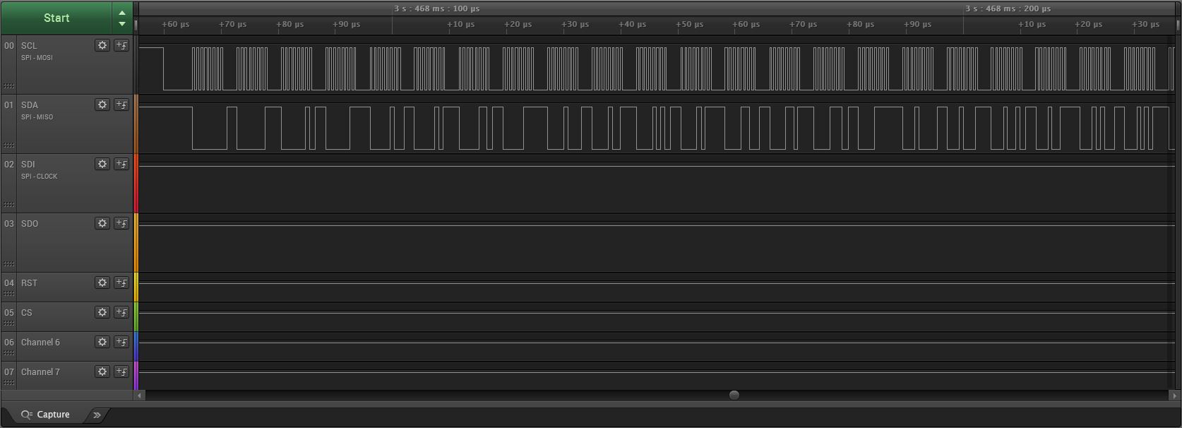
    Let me first thank you for your support and help and also let me apologize that I have not been careful enough not to notice the actual data being output. The scope was not set to trigger but free running; hence missed the actual data being output. Moreover was looking into it late night.

    Tested the code both with both 8bit and 32 bit mode as expected. Works with the DLB mode set also.

    For the sake of completion, I have attached a screenshot of the waveform:

    Tested with src wrap around too, works just as much as expected.

    Works beautifully, with all the tests.

    One additional question that I have:

    Let's suppose, I need to continuously run with src wrap; continuously outputting data. What could be done, if that's possible ?

    Thanks,

    Manu

  • Hi,

    You need to re-enable the channel inside the interrupt service routine of DMA end of transfer interrupt.

    Regards,
    Vivek Singh
  • Hi Vivek,

    Do you suggest to take the device out of the HALT state by RUN alone ? Or is something more necessary ?

    A simple RUN = 1, doesn't seem to be sufficient. On the contrary, it causes a side affect, where RUN=1, causes the erstwhile transfer to retrigger from the very beginning and the same procedure repeats itself.

    Thanks,

    Manu

  • Ah, sorry. Got mixed up, with another thread. Enabling RUN=1 causes the transfer to be continuous. Works as expected.

    Thanks,

    Manu