Part Number: TMS320F28376S
Other Parts Discussed in Thread: CONTROLSUITE
Dear community,
I have a problem receiving data from a Xilinx FPGA via the UPP bus. I programmed the protocol as described in http://www.ti.com/lit/ug/sprugj5b/sprugj5b.pdf on page 18.
Unfortunately I could not find any information about timings. The document only states:
- "By default, other signals align on the rising edge of CLOCK"
- "The active edge(s) of CLOCK should always slightly precede transitions of other uPP signals."
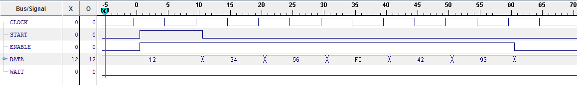
This is the simulated output from the FPGA with CLOCK, START, ENABLE (upper diagram) and 8-bit DATA (lower diagram):

I am trying to transmit 8 bytes of data in 1 line and 1 window. The clock frequency is 11 MHz.
The code on the C2000 is based on the ControlSuite example for UPP Reception. With the protocol realized as shown above, the controller does not trigger an interrupt. However, before this try I aligned the signals on the falling edge of the clock whereby I was able to generate an EOW (end of window) interrupt.
The problem was that when I analysed the memory at the address "uPP_RX_MSGRAM_ADDR" (0x6E00) it seemed like I only received 3 byte: D0, D2 and D4.
My questions now are:
- Why do I receive nothing when I use the timings stated in the UPP document ?
- Why are there only 3 bytes (from 6 specified in BYTE_CNT) in the UPP message RAM and it triggered the EOW interrupt ?
- What is the effect of "UppRegs.CHIDESC0 = 0x7000;" ? I expected the incoming data to be stored at that address but this memory is always empty.
I would be thankful for any advice!
Best regards, Josh
#include "F28x_Project.h"
#include "F2837xS_Upp_defines.h"

//
// Defines
//
#define LINE_CNT       1
#define BYTE_CNT       6
#define WIN_CNT        1
#define WIN_BYTE_CNT   6
#define WIN_WORD_CNT   3

//
// Globals
//
volatile long int ErrCount = 0;
volatile long int eow_int_cnt = 0;
volatile long int eol_int_cnt = 0;
volatile long int RdValue = 0;
volatile int CopyRxMsgRam = 0;
volatile long int DstAddr = 0xC000; // GS0 RAM

//
// Function Prototypes
//
extern void InitUpp1Gpio(void);
extern void SoftResetUpp(void);
interrupt void local_UPPA_ISR(void);

//
// Main
//
void main(void)
{
   int i;

//
// Initialize System Control
//
   InitSysCtrl();

   DINT;

   InitPieCtrl();

//
// Disable CPU interrupts and clear all CPU interrupt flags:
//
   EALLOW;
   IER = 0x0000;
   IFR = 0x0000;
   EDIS;

   InitPieVectTable();

   EALLOW;
   PieVectTable.UPPA_INT = &local_UPPA_ISR;

//
// Enable the Interrupt No 8.
//
   IER = M_INT8 ;

//
// Enable Interrupt for UPPA Interrupt.
//
   PieCtrlRegs.PIEIER8.bit.INTx15=1;

//
// Enable PIE & CPU level Interrupts.
//
   EnableInterrupts();

//
// Clear the RAM used for storing incoming data packet.
//
   MemCfgRegs.GSxINIT.bit.INIT_GS0 = 1;
   while (MemCfgRegs.GSxINITDONE.bit.INITDONE_GS0 == 0){};

//
// Issue SOFT Reset to uPP
//
   SoftResetUpp();


   InitGpio();
// Debug LED
   GPIO_SetupPinMux(93, GPIO_MUX_CPU1, 0);
   GPIO_SetupPinOptions(93, GPIO_OUTPUT, GPIO_PUSHPULL);

//
// Initialize UPP1 GPIO
//
   InitUpp1Gpio();

   GPIO_WritePin(93, 0);

//
// Configure uPP for RX
//
   UppRegs.IFCFG.bit.ENAA = 1;           //Use ENABLE Signal
   UppRegs.IFCFG.bit.STARTA = 1;         //Use START Signal
   //UppRegs.IFCFG.bit.WAITA = 1;
   UppRegs.CHCTL.bit.MODE = uPP_RX_MODE; // Setup for RX.
   UppRegs.CHCTL.bit.DRA = uPP_SDR;      // SDR mode

//
// Enable EOL/EOW interrupt
//
   UppRegs.INTENSET.bit.EOLI = 1;
   UppRegs.INTENSET.bit.EOWI = 1;
   UppRegs.GINTEN.bit.GINTEN = 1;

//
// Enable the uPP module
//
   UppRegs.PERCTL.bit.PEREN = 1;

//
// Setup DMA channel

//
   UppRegs.CHIDESC0 = 0x7000;
   UppRegs.CHIDESC1.bit.LCNT = LINE_CNT;
   UppRegs.CHIDESC1.bit.BCNT = BYTE_CNT;
   UppRegs.CHIDESC2.all = BYTE_CNT;

   while (eow_int_cnt < WIN_CNT);


   if(CopyRxMsgRam == 1)
   {
       if(eow_int_cnt%2)
       {
           for (i = 0; i < WIN_WORD_CNT ; i+=2)
           {
               RdValue = *(Uint32 *)(uPP_RX_MSGRAM_ADDR + WIN_WORD_CNT + i);
               *(Uint32 *)DstAddr = RdValue;
               DstAddr = DstAddr + 2;
           }
       }
       else
       {
           for (i = 0; i < WIN_WORD_CNT ; i+=2)
           {
               RdValue = *(Uint32 *)(uPP_RX_MSGRAM_ADDR + WIN_WORD_CNT + i);
               *(Uint32 *)DstAddr = RdValue;
               DstAddr = DstAddr + 2;
           }
       }
       CopyRxMsgRam = 0;
   }


//
// Disable the uPP to stop transmission after expected window count is done.
//
   UppRegs.PERCTL.bit.PEREN = 0;

//
// Issue SOFT Reset to uPP. This resets RX state machine but for that to happen,
// input clock (uPP_CLK) should be keep running.
// Hence issuing the reset here.
//
   SoftResetUpp();

   RdValue = 0;

   asm("          ESTOP0");
   for(;;);
}

//
// local_UPPA_ISR - UPPA Interrupt Service Routine (ISR)
//
interrupt void local_UPPA_ISR(void)
{
   int i;

   GPIO_WritePin(93, 1);

   //
   // To receive more interrupts from this PIE group, acknowledge
   // this interrupt
   //
   PieCtrlRegs.PIEACK.all = PIEACK_GROUP8;

   if (UppRegs.GINTFLG.all != 0x0)
   {
      if(UppRegs.ENINTST.bit.EOWI == 0x1) //Check for EOW Interrupt flag
      {
         eow_int_cnt++;
         CopyRxMsgRam = 1;

         //
         //Enable EOL interrupt
         //
         UppRegs.INTENSET.bit.EOLI = 1;

         //
         //Clear the Status for EOW Interrupt
         //
         UppRegs.ENINTST.all = uPP_INT_EOWI;

         if (UppRegs.ENINTST.bit.EOWI != 0)
         {
             ErrCount++;
             asm ("      ESTOP0");
         }
      }
      if(UppRegs.ENINTST.bit.EOLI == 0x1) // Check for EOL Interrupt Flag
      {
         eol_int_cnt++;

         //
         //Clear the Status and Disable EOL Interrupt
         //
         UppRegs.ENINTST.all = uPP_INT_EOLI;
         if (UppRegs.ENINTST.bit.EOLI != 0)
         {
             ErrCount++;
             asm ("      ESTOP0");
         }
         UppRegs.INTENCLR.all = uPP_INT_EOLI;
         if (UppRegs.INTENSET.bit.EOLI != 0)
         {
             ErrCount++;
             asm ("      ESTOP0");
         }

         //
         // Initialize the Channel Descriptor for Next window transfer.
         //


         if (eow_int_cnt < WIN_CNT)
         {
             if (eow_int_cnt%2)
             {
                 if(CopyRxMsgRam == 1)
                 {
                    for (i = 0; i < WIN_WORD_CNT ; i+=2)
                    {
                        RdValue = *(Uint32 *)(uPP_RX_MSGRAM_ADDR + i);
                        *(Uint32 *)DstAddr = RdValue;
                        DstAddr = DstAddr + 2;
                    }
                    CopyRxMsgRam = 0;
                 }
                 UppRegs.CHIDESC0 = 0x7000;
                 UppRegs.CHIDESC1.bit.LCNT = LINE_CNT;
                 UppRegs.CHIDESC1.bit.BCNT = BYTE_CNT;
                 UppRegs.CHIDESC2.all = BYTE_CNT;
             }
             else
             {
                 if(CopyRxMsgRam == 1)
                 {
                    for (i = 0; i < WIN_WORD_CNT ; i+=2)
                    {
                        RdValue = *(Uint32 *)(uPP_RX_MSGRAM_ADDR +
                                              WIN_WORD_CNT + i);
                        *(Uint32 *)DstAddr = RdValue;
                        DstAddr = DstAddr + 2;
                    }
                    CopyRxMsgRam = 0;
                 }
                 UppRegs.CHIDESC0 = 0x7000 + (LINE_CNT * BYTE_CNT);
                 UppRegs.CHIDESC1.bit.LCNT = LINE_CNT;
                 UppRegs.CHIDESC1.bit.BCNT = BYTE_CNT;
                 UppRegs.CHIDESC2.all = BYTE_CNT;
             }
         }


      }
      //
      // Clear Global Interrupt.
      //
      RdValue = UppRegs.ENINTST.all;
      UppRegs.GINTCLR.bit.GINTCLR = 1;
      if (UppRegs.GINTFLG.all != 0x0)
      {
         ErrCount++;
         asm ("      ESTOP0");
      }
   }
}