This thread has been locked.

If you have a related question, please click the "Ask a related question" button in the top right corner. The newly created question will be automatically linked to this question.

F28M35H52C: C28 Bootloader jump stuck in a forever loop inside _c_int00

Part Number: F28M35H52C


Hi guys,

Couple of months ago i was in conversation with Manoj one of the TI concerto device experts, taking his suggestions to resolve a problem i had back then which could be seen from the below post. 

A Recap of my previous post:

From the above link Manoj had suggested me to extract a copy of .dat file of memory locations at two different instances or steps. They are listed below:

Step1: Program C28x bootloader code and blinky code using JTAG and check whether C28x blinky code works when running in standalone mode. When I mean standalone mode, device should be disconnected from JTAG. 

Step2: Use M3 and C28 bootloader to program blinky code. If everything went correctly. Then C28x flash contents should be same as flash contents when using Step1.


In the previous post i collected .dat data with following settings

Format = Hex
Start Address = 0x100000
Memory Page = Data 
Length = 0x040000
Type-size = 16 bits

bootloader.dat

bootloader_afterblinky.dat

Back then there was a lot of differences in .dat file generated from step 1 and step 2. Which has been taken care now by some alterations i had to make in my C28 Bootloader project. 

A Summary of my current problem:

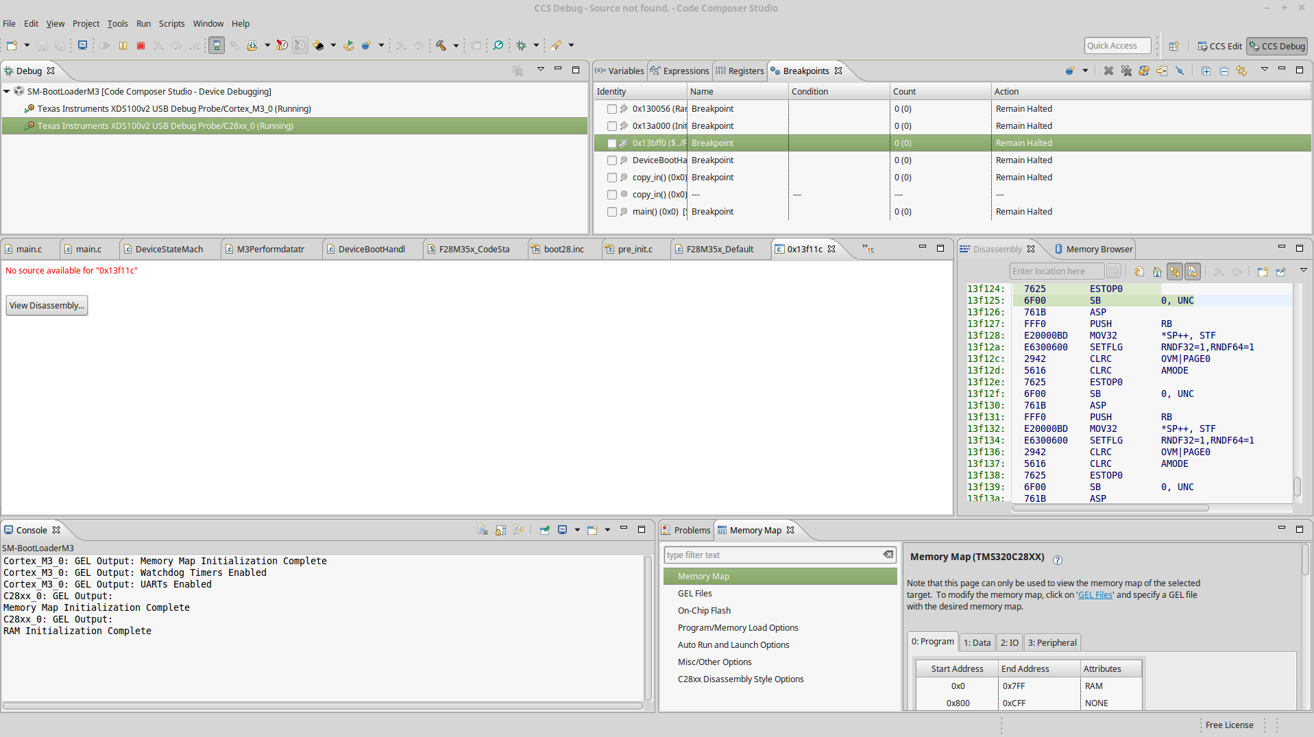
Now once i program the c28 blinky through my c28 bootloader and jump to the blinky "codestart" section(0x13A000) which is the start of _c_int00, i hit the breakpoint at 0x13A000 and step in to the _c_init00 function. A few steps further the program gets stuck in a forever loop and does not reach _copy_in (got the flow as per blinky .map file). 

In my previous post there was a complete reset after the jump but now i could atleast see that the reset is no more happening. Could i be missing sharing some resources between c28 bootloader and c28 blinky ? Or should i be aware of some initializations steps in my M3 Bootloader application which should transfer some resources to c28 blinky ? As of now i am sharing the GPIO resources for LED3 on concerto control card is this not sufficient enough ? 

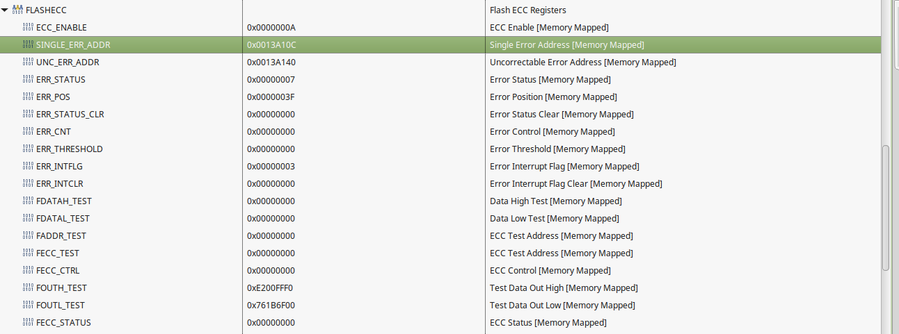
Some screen shots for References:

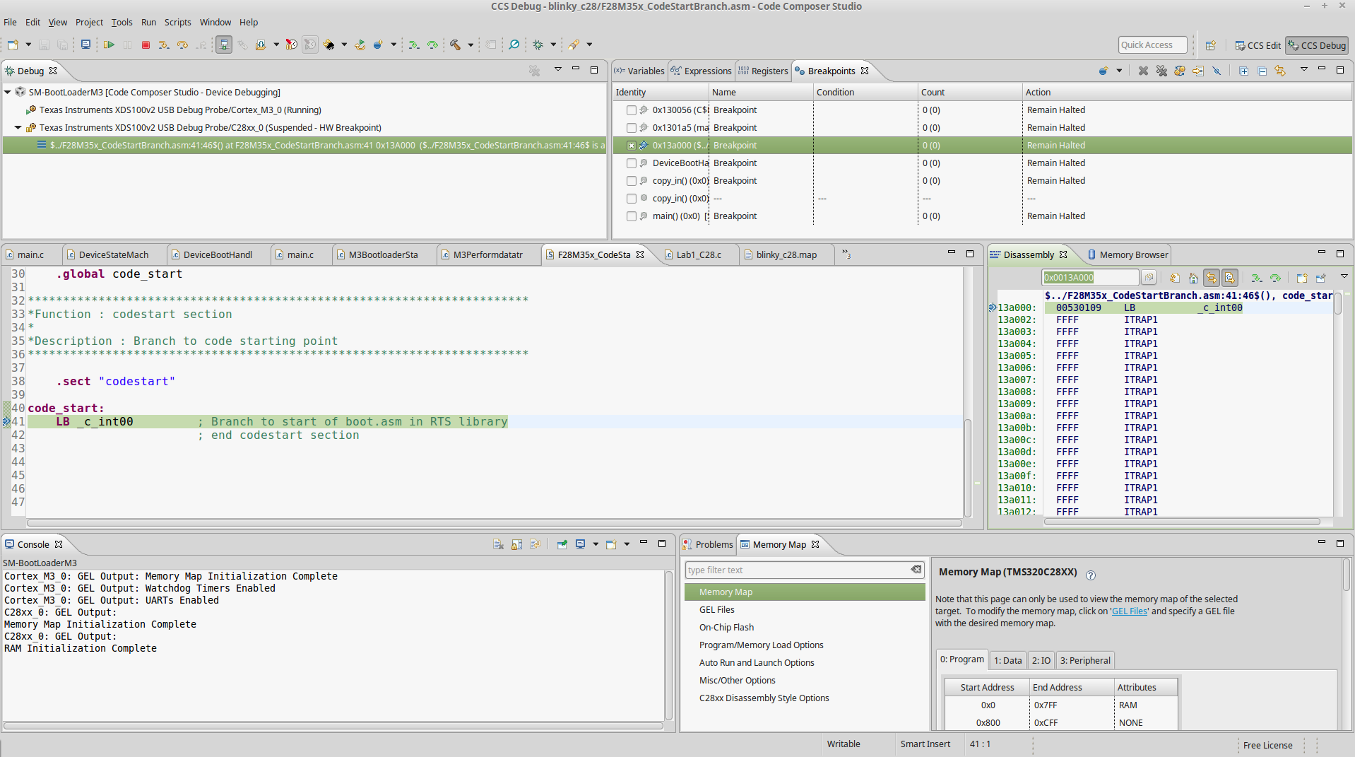
During the debugging session it halts in boot28.inc which i believe is part of TI library and can not be viewed. So how else could i trouble shoot this situation ? 

Thanks

  • Hello

    You should be able to find boot28 within the CCS installation and the compiler you are using.
    Ex: ~\ccsv8\tools\compiler\ti-cgt-c2000_18.1.3.LTS\lib\src

    Best regards
    Chris
  • Hi Christopher,

    Thanks for sharing this, it helped to troubleshoot by stepping through actual source code. 

    I made some changes on the linker script from c28 blinky application and currently my .cmd file for blinky is a attached below:

    /*
    //###########################################################################
    // FILE:    F28M35H52C1_c28.cmd
    // TITLE:    Linker Command File For F28M35H52C1 Device
    //###########################################################################
    // $TI Release: F28M35x Support Library v201 $
    // $Release Date: Fri Jun  7 10:51:13 CDT 2013 $
    //###########################################################################
    */
    
    /* ======================================================
    // For Code Composer Studio V2.2 and later
    // ---------------------------------------
    // In addition to this memory linker command file,
    // add the header linker command file directly to the project.
    // The header linker command file is required to link the
    // peripheral structures to the proper locations within
    // the memory map.
    // The header linker files are found in <base>\F28M35x_headers\cmd
    // For BIOS applications add:      F28M35x_Headers_BIOS.cmd
    // For nonBIOS applications add:   F28M35x_Headers_nonBIOS.cmd
    ========================================================= */
    
    /* Define the memory block start/length for the F28M35x
       PAGE 0 will be used to organize program sections
       PAGE 1 will be used to organize data sections
    
       Notes:
             Memory blocks on F28M35x are uniform (ie same
             physical memory) in both PAGE 0 and PAGE 1.
             That is the same memory region should not be
             defined for both PAGE 0 and PAGE 1.
             Doing so will result in corruption of program
             and/or data.
    
             Contiguous SARAM memory blocks or flash sectors can be
             be combined if required to create a larger memory block.
    */
    
    MEMORY
    {
    PAGE 0:    /* Program Memory */
               /* Memory (RAM/FLASH/OTP) blocks can be moved to PAGE1 for data allocation */
       RAML0       : origin = 0x008000, length = 0x001000     /* on-chip RAM block L0 */
       RAML1       : origin = 0x009000, length = 0x001000     /* on-chip RAM block L1 */
       
       FLASHN      : origin = 0x100000, length = 0x002000     /* on-chip FLASH */
       FLASHM      : origin = 0x102000, length = 0x002000     /* on-chip FLASH */
       FLASHL      : origin = 0x104000, length = 0x002000     /* on-chip FLASH */
       FLASHK      : origin = 0x106000, length = 0x002000     /* on-chip FLASH */
       FLASHJ      : origin = 0x108000, length = 0x008000     /* on-chip FLASH */
       FLASHI      : origin = 0x110000, length = 0x008000     /* on-chip FLASH */
       FLASHH      : origin = 0x118000, length = 0x008000     /* on-chip FLASH */
       FLASHG      : origin = 0x120000, length = 0x008000     /* on-chip FLASH */
       FLASHF      : origin = 0x128000, length = 0x008000     /* on-chip FLASH */
       FLASHE      : origin = 0x130000, length = 0x008000     /* on-chip FLASH */
       FLASHD      : origin = 0x138000, length = 0x002000     /* on-chip FLASH */
       FLASHC      : origin = 0x13A000, length = 0x001F80
       /*CSM_RSVD    : origin = 0x13BF80, length = 0x000070     /* Part of FLASHC.  Program with all 0x0000 when CSM is in use. */
       BEGIN       : origin = 0x13BFF0, length = 0x000002     /*0x002000*/
       /*FLASH_EXE_ONLY_P0  : origin = 0x13BFF2, length = 0x000002  /* Part of FLASHC.  Flash execute only locations in FLASHC */
       /*ECSL_PWL_P0 : origin = 0x13BFF4, length = 0x000004     /* Part of FLASHC.  ECSL password locations in FLASHC */
       /*CSM_PWL_P0  : origin = 0x13BFF8, length = 0x000008     /* Part of FLASHC.  CSM password locations in FLASHC */
    
    
       BOOTROM     : origin = 0x3FEDA8, length = 0x001200     /* Boot ROM */
       PIEMISHNDLR : origin = 0x3FFFBE, length = 0x000002     /* part of boot ROM  */
       RESET       : origin = 0x3FFFC0, length = 0x000002     /* part of boot ROM  */
       VECTORS     : origin = 0x3FFFC2, length = 0x00003E     /* part of boot ROM  */
    
    PAGE 1 :
       /* Data Memory */
               /* Memory (RAM/FLASH/OTP) blocks can be moved to PAGE0 for program allocation */
               /* Registers remain on PAGE1*/
    
       DEV_EMU             : origin = 0x000880, length = 0x000180     /* device emulation registers */
       CSM                 : origin = 0x000AE0, length = 0x000020       /* code security module registers */
    
       ADC1_RESULT         : origin = 0x000B00, length = 0x000020     /* ADC1 Results register */
       ADC2_RESULT         : origin = 0x000B40, length = 0x000020     /* ADC2 Results register */
    
       CPU_TIMER0          : origin = 0x000C00, length = 0x000008     /* CPU Timer0 registers */
       CPU_TIMER1          : origin = 0x000C08, length = 0x000008     /* CPU Timer1 registers */
       CPU_TIMER2          : origin = 0x000C10, length = 0x000008     /* CPU Timer2 registers */
    
       PIE_CTRL            : origin = 0x000CE0, length = 0x000020     /* PIE control registers */
       PIE_VECT            : origin = 0x000D00, length = 0x000100     /* PIE Vector Table */
       PIE_VECT_CP         : origin = 0x000E00, length = 0x000100     /* PIE Vector Table Copy */
    
       DMA                 : origin = 0x001000, length = 0x000200     /* DMA registers */
    
       ASYSCTRLCONFIG      : origin = 0x001700, length = 0x000080       /* Analog System Control Configuration Registers */
    
       /*HWBIST              : origin = 0x001780, length = 0x000040       /* HW BIST Registers    */
    
       FLASH_REGS          : origin = 0x004000, length = 0x000300     /* Flash Control registers */
       FLASH_ECC           : origin = 0x004300, length = 0x000040     /* Flash/OTP ECC Error Log registers */
    
       M3PLL               : origin = 0x004400, length = 0x000040       /* M3 PLL Clock Configuration Registers  */
    
       RAM_REGS            : origin = 0x004900, length = 0x000080     /* RAM Control registers */
       RAM_ERR_REGS        : origin = 0x004A00, length = 0x000080     /* RAM ECC/PARITY/ACCESS Error Log Registers */
    
       CM_MC_IPC           : origin = 0x004E00, length = 0x000040     /* C28 Control to Master IPC registers */
    
       MCBSPA              : origin = 0x005000, length = 0x000040     /* McBSP-A registers */
    
       EPWM1               : origin = 0x005100, length = 0x000080     /* EPWM1 + HRPWM registers */
       EPWM2               : origin = 0x005180, length = 0x000080     /* EPWM2 + HRPWM registers */
       EPWM3               : origin = 0x005200, length = 0x000080     /* EPWM3 + HRPWM registers */
       EPWM4               : origin = 0x005280, length = 0x000080     /* EPWM4 + HRPWM registers */
       EPWM5               : origin = 0x005300, length = 0x000080     /* EPWM5 + HRPWM registers */
       EPWM6               : origin = 0x005380, length = 0x000080     /* EPWM6 + HRPWM registers */
       EPWM7               : origin = 0x005400, length = 0x000080     /* EPWM7 + HRPWM registers */
       EPWM8               : origin = 0x005480, length = 0x000080     /* EPWM8 + HRPWM registers */
       EPWM9               : origin = 0x005500, length = 0x000080     /* EPWM9 registers */
    
       ECAP1               : origin = 0x005A00, length = 0x000020     /* Enhanced Capture 1 registers */
       ECAP2               : origin = 0x005A20, length = 0x000020     /* Enhanced Capture 2 registers */
       ECAP3               : origin = 0x005A40, length = 0x000020     /* Enhanced Capture 3 registers */
       ECAP4               : origin = 0x005A60, length = 0x000020     /* Enhanced Capture 4 registers */
       ECAP5               : origin = 0x005A80, length = 0x000020     /* Enhanced Capture 5 registers */
       ECAP6               : origin = 0x005AA0, length = 0x000020     /* Enhanced Capture 6 registers */
    
       EQEP1               : origin = 0x005B00, length = 0x000040     /* Enhanced QEP 1 registers */
       EQEP2               : origin = 0x005B40, length = 0x000040     /* Enhanced QEP 2 registers */
       EQEP3               : origin = 0x005B80, length = 0x000040     /* Enhanced QEP 3 registers */
    
       GPIOG1CTRL          : origin = 0x005F80, length = 0x000040     /* GPIO control registers */
       GPIOG1DAT           : origin = 0x005FC0, length = 0x000020     /* GPIO data registers */
       GPIOG1TRIP          : origin = 0x005FE0, length = 0x000020     /* GPIO trip/LPM registers */
    
       COMP1               : origin = 0x006400, length = 0x000020     /* Comparator + DAC 1 registers */
       COMP2               : origin = 0x006420, length = 0x000020     /* Comparator + DAC 2 registers */
       COMP3               : origin = 0x006440, length = 0x000020     /* Comparator + DAC 3 registers */
       COMP4               : origin = 0x006460, length = 0x000020     /* Comparator + DAC 4 registers */
       COMP5               : origin = 0x006480, length = 0x000020     /* Comparator + DAC 5 registers */
       COMP6               : origin = 0x0064A0, length = 0x000020     /* Comparator + DAC 6 registers */
    
       GPIOG2CTRL          : origin = 0x006F80, length = 0x000040     /* GPIO control registers */
       GPIOG2DAT           : origin = 0x006FC0, length = 0x000020     /* GPIO data registers */
    
       SYSTEM              : origin = 0x007010, length = 0x000020     /* System control registers */
    
       SPIA                : origin = 0x007040, length = 0x000010     /* SPI-A registers */\
       SCIA                : origin = 0x007050, length = 0x000010     /* SCI-A registers */
    
       NMIINTRUPT          : origin = 0x007060, length = 0x000010     /* NMI Watchdog Interrupt Registers */
       XINTRUPT            : origin = 0x007070, length = 0x000010     /* external interrupt registers */
    
       ADC1                : origin = 0x007100, length = 0x000080     /* ADC1 registers */
       ADC2                : origin = 0x007180, length = 0x000080     /* ADC2 registers */
    
       I2CA                : origin = 0x007900, length = 0x000040     /* I2C-A registers */
    
       FLASH_EXE_ONLY      : origin = 0x13FFF2, length = 0x000002       /* FLASH execution only locations */
       ECSL_PWL            : origin = 0x13FFF4, length = 0x000004       /* FLASH ECSL password locations  */
       CSM_PWL             : origin = 0x13FFF8, length = 0x000008     /* FLASH CSM password locations.  */
    
       /* RAM Memory */
       BOOT_RSVD   : origin = 0x000000, length = 0x000050     /* Part of M0, BOOT rom will use this for stack */
       RAMM0       : origin = 0x000050, length = 0x0003B0     /* on-chip RAM block M0 */
       RAMM1       : origin = 0x000400, length = 0x000400     /* on-chip RAM block M1 */
       RAML2       : origin = 0x00A000, length = 0x001000     /* on-chip RAM block L2 */
       RAML3       : origin = 0x00B000, length = 0x001000     /* on-chip RAM block L3 */
       RAMS0       : origin = 0x00C000, length = 0x001000     /* on-chip Shared RAM block S0 */
       RAMS1       : origin = 0x00D000, length = 0x001000     /* on-chip Shared RAM block S1 */
       RAMS2       : origin = 0x00E000, length = 0x001000     /* on-chip Shared RAM block S2 */
       RAMS3       : origin = 0x00F000, length = 0x001000     /* on-chip Shared RAM block S3 */
       RAMS4       : origin = 0x010000, length = 0x001000     /* on-chip Shared RAM block S4 */
       RAMS5       : origin = 0x011000, length = 0x001000     /* on-chip Shared RAM block S5 */
       RAMS6       : origin = 0x012000, length = 0x001000     /* on-chip Shared RAM block S6 */
       RAMS7       : origin = 0x013000, length = 0x001000     /* on-chip Shared RAM block S7 */
    
       CTOMRAM     : origin = 0x03F800, length = 0x000380     /* C28 to M3 Message RAM */
       MTOCRAM     : origin = 0x03FC00, length = 0x000380     /* M3 to C28 Message RAM */
    }
    
    /* Allocate sections to memory blocks.
       Note:
             codestart user defined section in DSP28_CodeStartBranch.asm used to redirect code
                       execution when booting to flash
             ramfuncs  user defined section to store functions that will be copied from Flash into RAM
    */
    
    SECTIONS
    {
    /*** PIE Vect Table and Boot ROM Variables Structures ***/
      UNION run = PIE_VECT, PAGE = 1
       {
          PieVectTableFile
          GROUP
          {
             EmuKeyVar
             EmuBModeVar
             FlashCallbackVar
             FlashScalingVar
          }
       }
    
       /* Allocate program areas: */
       .cinit              : > FLASHC,      PAGE = 0, ALIGN(4)
       .pinit              : > FLASHC,      PAGE = 0, ALIGN(4)
       .text               : > FLASHC,      PAGE = 0, ALIGN(4)
       codestart           : > BEGIN,       PAGE = 0, ALIGN(4)
       ramfuncs            : LOAD = FLASHC,
                             RUN = RAML1,
                             LOAD_START(_RamfuncsLoadStart),
                             LOAD_SIZE(_RamfuncsLoadSize),
                             LOAD_END(_RamfuncsLoadEnd),
                             RUN_START(_RamfuncsRunStart),
                             RUN_SIZE(_RamfuncsRunSize),
                             RUN_END(_RamfuncsRunEnd),
                             PAGE = 0, ALIGN(4)
    
       /*flashexeonly        : > FLASH_EXE_ONLY_P0 PAGE = 0, ALIGN(4)
       ecslpasswds         : > ECSL_PWL_P0 PAGE = 0, ALIGN(4)
       csmpasswds          : > CSM_PWL_P0  PAGE = 0, ALIGN(4)
       csm_rsvd            : > CSM_RSVD    PAGE = 0, ALIGN(4)*/
    
       /*** Peripheral Frame 0 Register Structures ***/
       DevEmuRegsFile       : > DEV_EMU,     PAGE = 1
       CsmRegsFile          : > CSM,         PAGE = 1
       UNION run =              ADC1_RESULT, PAGE = 1
       {
           AdcResultFile
           Adc1ResultFile
       }
       Adc2ResultFile        : > ADC2_RESULT,     PAGE = 1
       CpuTimer0RegsFile     : > CPU_TIMER0,      PAGE = 1
       CpuTimer1RegsFile     : > CPU_TIMER1,      PAGE = 1
       CpuTimer2RegsFile     : > CPU_TIMER2,      PAGE = 1
       PieCtrlRegsFile       : > PIE_CTRL,        PAGE = 1
       PieVectTableCopyFile  : > PIE_VECT_CP,     PAGE = 1
       DmaRegsFile           : > DMA,             PAGE = 1
       AnalogSysctrlRegsFile : > ASYSCTRLCONFIG,  PAGE = 1
       /*HWBistRegsFile         : > HWBIST,         PAGE = 1
    
    /*** Peripheral Frame 1 Register Structures ***/
       FlashCtrlRegsFile : > FLASH_REGS,  PAGE = 1
       FlashEccRegsFile  : > FLASH_ECC,   PAGE = 1
       M3PllRegsFile     : > M3PLL,       PAGE = 1
       RAMRegsFile       : > RAM_REGS,    PAGE = 1
       RAMErrRegsFile    : > RAM_ERR_REGS,PAGE = 1
       CtoMIpcRegsFile   : > CM_MC_IPC,   PAGE = 1
       
    /*** Peripheral Frame 2 Register Structures ***/
       SysCtrlRegsFile   : > SYSTEM,      PAGE = 1
       SpiaRegsFile      : > SPIA,        PAGE = 1
       SciaRegsFile      : > SCIA,        PAGE = 1
       NmiIntruptRegsFile: > NMIINTRUPT,  PAGE = 1
       XIntruptRegsFile  : > XINTRUPT,    PAGE = 1
       UNION run =           ADC1,        PAGE = 1
       {
           AdcRegsFile
           Adc1RegsFile
       }
       Adc2RegsFile      : > ADC2,        PAGE = 1
       I2caRegsFile      : > I2CA,        PAGE = 1
    
    /*** Peripheral Frame 3 Register Structures ***/
       McbspaRegsFile    : > MCBSPA,      PAGE = 1
       EPwm1RegsFile     : > EPWM1,       PAGE = 1
       EPwm2RegsFile     : > EPWM2,       PAGE = 1
       EPwm3RegsFile     : > EPWM3,       PAGE = 1
       EPwm4RegsFile     : > EPWM4,       PAGE = 1
       EPwm5RegsFile     : > EPWM5,       PAGE = 1
       EPwm6RegsFile     : > EPWM6,       PAGE = 1
       EPwm7RegsFile     : > EPWM7,       PAGE = 1
       EPwm8RegsFile     : > EPWM8,       PAGE = 1
       EPwm9RegsFile     : > EPWM9,       PAGE = 1
       ECap1RegsFile     : > ECAP1,       PAGE = 1
       ECap2RegsFile     : > ECAP2,       PAGE = 1
       ECap3RegsFile     : > ECAP3,       PAGE = 1
       ECap4RegsFile     : > ECAP4,       PAGE = 1
       ECap5RegsFile     : > ECAP5,       PAGE = 1
       ECap6RegsFile     : > ECAP6,       PAGE = 1
       EQep1RegsFile     : > EQEP1,       PAGE = 1
       EQep2RegsFile     : > EQEP2,       PAGE = 1
       EQep3RegsFile     : > EQEP3,       PAGE = 1
       UNION run =           GPIOG1CTRL,  PAGE = 1
       {
           GpioCtrlRegsFile
           GpioG1CtrlRegsFile
       }
       UNION run =           GPIOG1DAT,  PAGE = 1
       {
           GpioDataRegsFile
           GpioG1DataRegsFile
       }
       UNION run =           GPIOG1TRIP,  PAGE = 1
       {
           GpioTripRegsFile
           GpioG1TripRegsFile
       }
    
       Comp1RegsFile      : > COMP1,       PAGE = 1
       Comp2RegsFile      : > COMP2,       PAGE = 1
       Comp3RegsFile      : > COMP3,       PAGE = 1
       Comp4RegsFile      : > COMP4,       PAGE = 1
       Comp5RegsFile      : > COMP5,       PAGE = 1
       Comp6RegsFile      : > COMP6,       PAGE = 1
       GpioG2CtrlRegsFile : > GPIOG2CTRL,  PAGE = 1
       GpioG2DataRegsFile : > GPIOG2DAT,   PAGE = 1
       /* The following section definitions are required when using the IPC API Drivers */ 
       GROUP : > CTOMRAM, PAGE = 1
       {
           PUTBUFFER 
           PUTWRITEIDX 
           GETREADIDX 
       }
    
       GROUP : > MTOCRAM, PAGE = 1
       {
           GETBUFFER :    TYPE = DSECT
           GETWRITEIDX :  TYPE = DSECT
           PUTREADIDX :   TYPE = DSECT
       }   
       
       /* Allocate uninitalized data sections: */
       .stack              : > RAMM0       PAGE = 1
       .ebss               : > RAML2       PAGE = 1
       .esysmem            : > RAML2       PAGE = 1
    
       /* Initalized sections go in Flash */
       /* For SDFlash to program these, they must be allocated to page 0 */
       .econst             : > FLASHC,      PAGE = 0, ALIGN(4)
       .switch             : > FLASHC,      PAGE = 0, ALIGN(4)
    
       /* .reset is a standard section used by the compiler.  It contains the */
       /* the address of the start of _c_int00 for C Code.   /*
       /* When using the boot ROM this section and the CPU vector */
       /* table is not needed.  Thus the default type is set here to  */
       /* DSECT  */
       .reset              : > RESET,      PAGE = 0, TYPE = DSECT, ALIGN(4)
       vectors             : > VECTORS,     PAGE = 0, TYPE = DSECT, ALIGN(4)
    
       /*** Code Security Module Register Structures ***/
       FlashExeOnlyFile  : > FLASH_EXE_ONLY,      PAGE = 1
       EcslPwlFile       : > ECSL_PWL,            PAGE = 1
       CsmPwlFile        : > CSM_PWL,             PAGE = 1
    
    }
    
    /*
    */


    And the .cmd file i am using for my C28 bootloader code is attached below:

    /*
    //###########################################################################
    // FILE:    F28M35H52C1_c28.cmd
    // TITLE:    Linker Command File For F28M35H52C1 Device
    //###########################################################################
    // $TI Release: F28M35x Support Library v201 $
    // $Release Date: Fri Jun  7 10:51:13 CDT 2013 $
    //###########################################################################
    */
    
    /* ======================================================
    // For Code Composer Studio V2.2 and later
    // ---------------------------------------
    // In addition to this memory linker command file,
    // add the header linker command file directly to the project.
    // The header linker command file is required to link the
    // peripheral structures to the proper locations within
    // the memory map.
    // The header linker files are found in <base>\F28M35x_headers\cmd
    // For BIOS applications add:      F28M35x_Headers_BIOS.cmd
    // For nonBIOS applications add:   F28M35x_Headers_nonBIOS.cmd
    ========================================================= */
    
    /* Define the memory block start/length for the F28M35x
       PAGE 0 will be used to organize program sections
       PAGE 1 will be used to organize data sections
    
       Notes:
             Memory blocks on F28M35x are uniform (ie same
             physical memory) in both PAGE 0 and PAGE 1.
             That is the same memory region should not be
             defined for both PAGE 0 and PAGE 1.
             Doing so will result in corruption of program
             and/or data.
    
             Contiguous SARAM memory blocks or flash sectors can be
             be combined if required to create a larger memory block.
    */
    
    MEMORY
    {
    PAGE 0:    /* Program Memory */
               /* Memory (RAM/FLASH/OTP) blocks can be moved to PAGE1 for data allocation */
       RAML0       : origin = 0x008000, length = 0x001000     /* on-chip RAM block L0 */
       RAML1       : origin = 0x009000, length = 0x001000     /* on-chip RAM block L1 */
       
       CSM_PWL_P0  : origin = 0x13FFF8, length = 0x000008     /* Part of FLASHA.  CSM password locations in FLASHA */
       ECSL_PWL_P0 : origin = 0x13FFF4, length = 0x000004     /* Part of FLASHA.  ECSL password locations in FLASHA */
       FLASH_EXE_ONLY_P0  : origin = 0x13FFF2, length = 0x000002  /* Part of FLASHA.  Flash execute only locations in FLASHA */
       BEGIN       : origin = 0x13FFF0, length = 0x000002	  /* Part of FLASHA.  Used for "boot to Flash" bootloader mode. */
       CSM_RSVD    : origin = 0x13FF80, length = 0x000070     /* Part of FLASHA.  Program with all 0x0000 when CSM is in use. */
       FLASHA      : origin = 0x13E000, length = 0x001F80      /* on-chip FLASH */
       FLASHB      : origin = 0x13C000, length = 0x002000     /* on-chip FLASH */
    
       FPUTABLES   : origin = 0x3FD258, length = 0x0006A0      /* FPU Tables in Boot ROM */
       IQTABLES    : origin = 0x3FD8F8, length = 0x000B50      /* IQ Math Tables in Boot ROM */
       IQTABLES2   : origin = 0x3FE448, length = 0x00008C      /* IQ Math Tables in Boot ROM */
       IQTABLES3   : origin = 0x3FE4D4, length = 0x0000AA      /* IQ Math Tables in Boot ROM */
    
       BOOTROM     : origin = 0x3FEDA8, length = 0x001200      /* Boot ROM */
       PIEMISHNDLR : origin = 0x3FFFBE, length = 0x000002      /* part of boot ROM  */
       RESET       : origin = 0x3FFFC0, length = 0x000002      /* part of boot ROM  */
       VECTORS     : origin = 0x3FFFC2, length = 0x00003E      /* part of boot ROM  */
    
    PAGE 1 :   /* Data Memory */
               /* Memory (RAM/FLASH/OTP) blocks can be moved to PAGE0 for program allocation */
               /* Registers remain on PAGE1                                                  */
    
       /*C28 Pheripheral Register Memory Region*/
    
       PIE_CTRL            : origin = 0x000CE0, length = 0x000020     /* PIE control registers */
       PIE_VECT            : origin = 0x000D00, length = 0x000100     /* PIE Vector Table */
       PIE_VECT_CP         : origin = 0x000E00, length = 0x000100     /* PIE Vector Table Copy */
    
       DEV_EMU             : origin = 0x000880, length = 0x000180     /* device emulation registers */
       CSM                 : origin = 0x000AE0, length = 0x000020       /* code security module registers */
    
       ADC1_RESULT         : origin = 0x000B00, length = 0x000020     /* ADC1 Results register */
       ADC2_RESULT         : origin = 0x000B40, length = 0x000020     /* ADC2 Results register */
    
       CPU_TIMER0          : origin = 0x000C00, length = 0x000008     /* CPU Timer0 registers */
       CPU_TIMER1          : origin = 0x000C08, length = 0x000008     /* CPU Timer1 registers */
       CPU_TIMER2          : origin = 0x000C10, length = 0x000008     /* CPU Timer2 registers */
    
       DMA                 : origin = 0x001000, length = 0x000200     /* DMA registers */
    
       ASYSCTRLCONFIG      : origin = 0x001700, length = 0x000080       /* Analog System Control Configuration Registers */
    
       FLASH_REGS          : origin = 0x004000, length = 0x000300     /* Flash Control registers */
       FLASH_ECC           : origin = 0x004300, length = 0x000040     /* Flash/OTP ECC Error Log registers */
    
       M3PLL               : origin = 0x004400, length = 0x000010       /* M3 PLL Clock Configuration Registers  */
    
       EPI_REGS            : origin = 0x004430, length = 0x000010       /* EPI Registers  */
    
       RAM_REGS            : origin = 0x004900, length = 0x000080     /* RAM Control registers */
       RAM_ERR_REGS        : origin = 0x004A00, length = 0x000080     /* RAM ECC/PARITY/ACCESS Error Log Registers */
    
       CM_MC_IPC   : origin = 0x004E00, length = 0x000040     /* C28 Control to Master IPC registers */
    
       MCBSPA              : origin = 0x005000, length = 0x000040     /* McBSP-A registers */
    
       EPWM1               : origin = 0x005100, length = 0x000080     /* EPWM1 + HRPWM registers */
       EPWM2               : origin = 0x005180, length = 0x000080     /* EPWM2 + HRPWM registers */
       EPWM3               : origin = 0x005200, length = 0x000080     /* EPWM3 + HRPWM registers */
       EPWM4               : origin = 0x005280, length = 0x000080     /* EPWM4 + HRPWM registers */
       EPWM5               : origin = 0x005300, length = 0x000080     /* EPWM5 + HRPWM registers */
       EPWM6               : origin = 0x005380, length = 0x000080     /* EPWM6 + HRPWM registers */
       EPWM7               : origin = 0x005400, length = 0x000080     /* EPWM7 + HRPWM registers */
       EPWM8               : origin = 0x005480, length = 0x000080     /* EPWM8 + HRPWM registers */
       EPWM9               : origin = 0x005500, length = 0x000080     /* EPWM9 registers (no HRPWM) */
    
       ECAP1               : origin = 0x005A00, length = 0x000020     /* Enhanced Capture 1 registers */
       ECAP2               : origin = 0x005A20, length = 0x000020     /* Enhanced Capture 2 registers */
       ECAP3               : origin = 0x005A40, length = 0x000020     /* Enhanced Capture 3 registers */
       ECAP4               : origin = 0x005A60, length = 0x000020     /* Enhanced Capture 4 registers */
       ECAP5               : origin = 0x005A80, length = 0x000020     /* Enhanced Capture 5 registers */
       ECAP6               : origin = 0x005AA0, length = 0x000020     /* Enhanced Capture 6 registers */
    
       EQEP1               : origin = 0x005B00, length = 0x000040     /* Enhanced QEP 1 registers */
       EQEP2               : origin = 0x005B40, length = 0x000040     /* Enhanced QEP 2 registers */
       EQEP3               : origin = 0x005B80, length = 0x000040     /* Enhanced QEP 3 registers */
    
       GPIOG1CTRL          : origin = 0x005F80, length = 0x000040     /* GPIO control registers */
       GPIOG1DAT           : origin = 0x005FC0, length = 0x000020     /* GPIO data registers */
       GPIOG1TRIP          : origin = 0x005FE0, length = 0x000020     /* GPIO trip/LPM registers */
    
       COMP1               : origin = 0x006400, length = 0x000020     /* Comparator + DAC 1 registers */
       COMP2               : origin = 0x006420, length = 0x000020     /* Comparator + DAC 2 registers */
       COMP3               : origin = 0x006440, length = 0x000020     /* Comparator + DAC 3 registers */
       COMP4               : origin = 0x006460, length = 0x000020     /* Comparator + DAC 4 registers */
       COMP5               : origin = 0x006480, length = 0x000020     /* Comparator + DAC 5 registers */
       COMP6               : origin = 0x0064A0, length = 0x000020     /* Comparator + DAC 6 registers */
    
       GPIOG2CTRL          : origin = 0x006F80, length = 0x000040     /* GPIO control registers */
       GPIOG2DAT           : origin = 0x006FC0, length = 0x000020     /* GPIO data registers */
    
       SYSTEM              : origin = 0x007010, length = 0x000020     /* System control registers */
    
       SPIA                : origin = 0x007040, length = 0x000010     /* SPI-A registers */
       SCIA                : origin = 0x007050, length = 0x000010     /* SCI-A registers */
    
       NMIINTRUPT          : origin = 0x007060, length = 0x000010     /* NMI Watchdog Interrupt Registers */
       XINTRUPT            : origin = 0x007070, length = 0x000010     /* external interrupt registers */
    
       ADC1                : origin = 0x007100, length = 0x000080     /* ADC1 registers */
       ADC2                : origin = 0x007180, length = 0x000080     /* ADC2 registers */
    
       I2CA                : origin = 0x007900, length = 0x000040     /* I2C-A registers */
    
       /*End of C28 Pheripheral region and start of RAM section*/
    
       /* RAM Memory */
       BOOT_RSVD   : origin = 0x000000, length = 0x000050     /* Part of M0, BOOT rom will use this for stack */
       RAMM0       : origin = 0x000050, length = 0x0003B0     /* on-chip RAM block M0 */
       RAMM1       : origin = 0x000400, length = 0x000400     /* on-chip RAM block M1 */
       RAML2       : origin = 0x00A000, length = 0x001000     /* on-chip RAM block L2 */
       RAML3       : origin = 0x00B000, length = 0x001000     /* on-chip RAM block L3 */
       RAMS0       : origin = 0x00C000, length = 0x001000     /* on-chip Shared RAM block S0 */
       RAMS1       : origin = 0x00D000, length = 0x001000     /* on-chip Shared RAM block S1 */
       RAMS2       : origin = 0x00E000, length = 0x001000     /* on-chip Shared RAM block S2 */
       RAMS3       : origin = 0x00F000, length = 0x001000     /* on-chip Shared RAM block S3 */
       RAMS4       : origin = 0x010000, length = 0x001000     /* on-chip Shared RAM block S4 */
       RAMS5       : origin = 0x011000, length = 0x001000     /* on-chip Shared RAM block S5 */
       RAMS6       : origin = 0x012000, length = 0x001000     /* on-chip Shared RAM block S6 */
       RAMS7       : origin = 0x013000, length = 0x001000     /* on-chip Shared RAM block S7 */
    
       CTOMRAM     : origin = 0x03F800, length = 0x000380     /* C28 to M3 Message RAM */
       MTOCRAM     : origin = 0x03FC00, length = 0x000380     /* M3 to C28 Message RAM */
    
       FLASH_EXE_ONLY      : origin = 0x13FFF2, length = 0x000002       /* FLASH execution only locations */
       ECSL_PWL            : origin = 0x13FFF4, length = 0x000004       /* FLASH ECSL password locations  */
       CSM_PWL             : origin = 0x13FFF8, length = 0x000008     /* FLASH CSM password locations.  */
    }
    
    /* Allocate sections to memory blocks.
       Note:
             codestart user defined section in DSP28_CodeStartBranch.asm used to redirect code
                       execution when booting to flash
             ramfuncs  user defined section to store functions that will be copied from Flash into RAM
    */
    
    SECTIONS
    {
    
    /*** PIE Vect Table and Boot ROM Variables Structures ***/
      UNION run = PIE_VECT, PAGE = 1
       {
          PieVectTableFile
          GROUP
          {
             EmuKeyVar
             EmuBModeVar
             FlashCallbackVar
             FlashScalingVar
          }
       }
    
       /* Allocate program areas: */
       .cinit              : > FLASHA,      PAGE = 0, ALIGN(4)
       .pinit              : > FLASHA,      PAGE = 0, ALIGN(4)
       .text               : > FLASHA,      PAGE = 0, ALIGN(4)
       codestart           : > BEGIN,       PAGE = 0, ALIGN(4)
    
    #ifdef __TI_COMPILER_VERSION__
        #if __TI_COMPILER_VERSION__ >= 15009000
            GROUP
            {
                .TI.ramfunc
                { -l F021_API_C28x_FPU32.lib}
    
            } LOAD = FLASHA,
              RUN = RAML0,
              LOAD_START(_RamfuncsLoadStart),
              LOAD_SIZE(_RamfuncsLoadSize),
              RUN_START(_RamfuncsRunStart),
              PAGE = 0, ALIGN(4)
        #else
            GROUP
            {
                ramfuncs
                { -l F021_API_C28x_FPU32.lib}
    
            } LOAD = FLASHA,
              RUN = RAML0,
              LOAD_START(_RamfuncsLoadStart),
              LOAD_SIZE(_RamfuncsLoadSize),
              RUN_START(_RamfuncsRunStart),
              PAGE = 0, ALIGN(4)
        #endif
    #endif
    
       flashexeonly        : > FLASH_EXE_ONLY_P0 PAGE = 0, ALIGN(4)
       ecslpasswds         : > ECSL_PWL_P0 PAGE = 0, ALIGN(4)
       csmpasswds          : > CSM_PWL_P0  PAGE = 0, ALIGN(4)
       csm_rsvd            : > CSM_RSVD    PAGE = 0, ALIGN(4)
    
    /*** Peripheral Frame 0 Register Structures ***/
       DevEmuRegsFile       : > DEV_EMU,     PAGE = 1
       CsmRegsFile          : > CSM,         PAGE = 1
       UNION run =              ADC1_RESULT, PAGE = 1
       {
           AdcResultFile
           Adc1ResultFile
       }
       Adc2ResultFile        : > ADC2_RESULT,     PAGE = 1
       CpuTimer0RegsFile     : > CPU_TIMER0,      PAGE = 1
       CpuTimer1RegsFile     : > CPU_TIMER1,      PAGE = 1
       CpuTimer2RegsFile     : > CPU_TIMER2,      PAGE = 1
       PieCtrlRegsFile       : > PIE_CTRL,        PAGE = 1
       PieVectTableCopyFile  : > PIE_VECT_CP,     PAGE = 1
       DmaRegsFile           : > DMA,             PAGE = 1
       AnalogSysctrlRegsFile : > ASYSCTRLCONFIG,  PAGE = 1
    
    /*** Peripheral Frame 1 Register Structures ***/
       FlashCtrlRegsFile : > FLASH_REGS,  PAGE = 1
       FlashEccRegsFile  : > FLASH_ECC,   PAGE = 1
       M3PllRegsFile     : > M3PLL,       PAGE = 1
       EpiRegsFile       : > EPI_REGS     PAGE = 1
       RAMRegsFile       : > RAM_REGS,    PAGE = 1
       RAMErrRegsFile    : > RAM_ERR_REGS,PAGE = 1
       CtoMIpcRegsFile   : > CM_MC_IPC,   PAGE = 1
       
    /*** Peripheral Frame 2 Register Structures ***/
       SysCtrlRegsFile   : > SYSTEM,      PAGE = 1
       SpiaRegsFile      : > SPIA,        PAGE = 1
       SciaRegsFile      : > SCIA,        PAGE = 1
       NmiIntruptRegsFile: > NMIINTRUPT,  PAGE = 1
       XIntruptRegsFile  : > XINTRUPT,    PAGE = 1
       UNION run =           ADC1,        PAGE = 1
       {
           AdcRegsFile
           Adc1RegsFile
       }
       Adc2RegsFile      : > ADC2,        PAGE = 1
       I2caRegsFile      : > I2CA,        PAGE = 1
    
    /*** Peripheral Frame 3 Register Structures ***/
       McbspaRegsFile    : > MCBSPA,      PAGE = 1
       EPwm1RegsFile     : > EPWM1,       PAGE = 1
       EPwm2RegsFile     : > EPWM2,       PAGE = 1
       EPwm3RegsFile     : > EPWM3,       PAGE = 1
       EPwm4RegsFile     : > EPWM4,       PAGE = 1
       EPwm5RegsFile     : > EPWM5,       PAGE = 1
       EPwm6RegsFile     : > EPWM6,       PAGE = 1
       EPwm7RegsFile     : > EPWM7,       PAGE = 1
       EPwm8RegsFile     : > EPWM8,       PAGE = 1
       EPwm9RegsFile     : > EPWM9,       PAGE = 1
       ECap1RegsFile     : > ECAP1,       PAGE = 1
       ECap2RegsFile     : > ECAP2,       PAGE = 1
       ECap3RegsFile     : > ECAP3,       PAGE = 1
       ECap4RegsFile     : > ECAP4,       PAGE = 1
       ECap5RegsFile     : > ECAP5,       PAGE = 1
       ECap6RegsFile     : > ECAP6,       PAGE = 1
       EQep1RegsFile     : > EQEP1,       PAGE = 1
       EQep2RegsFile     : > EQEP2,       PAGE = 1
       EQep3RegsFile     : > EQEP3,       PAGE = 1
       UNION run =           GPIOG1CTRL,  PAGE = 1
       {
           GpioCtrlRegsFile
           GpioG1CtrlRegsFile
       }
       UNION run =           GPIOG1DAT,  PAGE = 1
       {
           GpioDataRegsFile
           GpioG1DataRegsFile
       }
       UNION run =           GPIOG1TRIP,  PAGE = 1
       {
           GpioTripRegsFile
           GpioG1TripRegsFile
       }
    
       Comp1RegsFile      : > COMP1,       PAGE = 1
       Comp2RegsFile      : > COMP2,       PAGE = 1
       Comp3RegsFile      : > COMP3,       PAGE = 1
       Comp4RegsFile      : > COMP4,       PAGE = 1
       Comp5RegsFile      : > COMP5,       PAGE = 1
       Comp6RegsFile      : > COMP6,       PAGE = 1
       GpioG2CtrlRegsFile : > GPIOG2CTRL,  PAGE = 1
       GpioG2DataRegsFile : > GPIOG2DAT,   PAGE = 1
    
       /* The following section definitions are required when using the IPC API Drivers */ 
    
       GROUP : > CTOMRAM, PAGE = 1 
       {
           PUTBUFFER 
           PUTWRITEIDX 
           GETREADIDX 
       }
    
       GROUP : > MTOCRAM, PAGE = 1
       {
           GETBUFFER :    TYPE = DSECT
           GETWRITEIDX :  TYPE = DSECT
           PUTREADIDX :   TYPE = DSECT
       }   
       
       /* Allocate uninitalized data sections: */
       .stack              : > RAMM0       PAGE = 1
       .ebss               : > RAML2       PAGE = 1
       .esysmem            : > RAML2       PAGE = 1
    
       /* Initalized sections go in Flash */
       /* For SDFlash to program these, they must be allocated to page 0 */
       .econst             : > FLASHA      PAGE = 0, ALIGN(4)
       .switch             : > FLASHA      PAGE = 0, ALIGN(4)
    
       /* Allocate IQ math areas: */
       IQmath              : > FLASHA      PAGE = 0 , ALIGN(4)           /* Math Code */
       IQmathTables        : > IQTABLES,   PAGE = 0, TYPE = NOLOAD, ALIGN(4)
    
       /* Allocate FPU math areas: */
       FPUmathTables       : > FPUTABLES,  PAGE = 0, TYPE = NOLOAD, ALIGN(4)
       
       DMARAML2           : > RAML2,       PAGE = 1
       DMARAML3           : > RAML3,       PAGE = 1
    
      /* Uncomment the section below if calling the IQNexp() or IQexp()
          functions from the IQMath.lib library in order to utilize the
          relevant IQ Math table in Boot ROM (This saves space and Boot ROM
          is 1 wait-state). If this section is not uncommented, IQmathTables2
          will be loaded into other memory (SARAM, Flash, etc.) and will take
          up space, but 0 wait-state is possible.
       */
       /*
       IQmathTables2    : > IQTABLES2, PAGE = 0, TYPE = NOLOAD
       {
    
                  IQmath.lib<IQNexpTable.obj> (IQmathTablesRam)
    
       }
       */
        /* Uncomment the section below if calling the IQNasin() or IQasin()
           functions from the IQMath.lib library in order to utilize the
           relevant IQ Math table in Boot ROM (This saves space and Boot ROM
           is 1 wait-state). If this section is not uncommented, IQmathTables2
           will be loaded into other memory (SARAM, Flash, etc.) and will take
           up space, but 0 wait-state is possible.
        */
        /*
        IQmathTables3    : > IQTABLES3, PAGE = 0, TYPE = NOLOAD
        {
    
                   IQmath.lib<IQNasinTable.obj> (IQmathTablesRam)
    
        }
        */
    
       /* .reset is a standard section used by the compiler.  It contains the */
       /* the address of the start of _c_int00 for C Code.   /*
       /* When using the boot ROM this section and the CPU vector */
       /* table is not needed.  Thus the default type is set here to  */
       /* DSECT  */
       .reset              : > RESET,      PAGE = 0, TYPE = DSECT, ALIGN(4)
       vectors             : > VECTORS,     PAGE = 0, TYPE = DSECT, ALIGN(4)
    
    
       /*** Code Security Module Register Structures ***/
       FlashExeOnlyFile  : > FLASH_EXE_ONLY,      PAGE = 1
       EcslPwlFile       : > ECSL_PWL,            PAGE = 1
       CsmPwlFile        : > CSM_PWL,             PAGE = 1
    }
    
    /*
    */


    I am using FLASH A and FLASH B for my Bootloader application and rest of the FLASH sectors for the blinky application. However both the application specify the MEMORY and SECTIONS for different peripheral regions which i picked up some control suite examples. Now is this valid or should i specify peripheral MEMORY and SECTIONS in any one of them ?

    Now as part of trouble shooting i performed two different steps as explained below:

    1. I flashed my M3 Bootloader and C28 Bootloader and programmed C28 Blinky through the C28 Bootloader expecting something to happen. Now i see a different behavior compared to what i explain in my first post. Here when i get in to first instruction under START: routine inside boot28.inc  and step into i end up in a invalid address jump to address 0x13f11c. Below are some screenshots explaining this behavior. 

      Here the XAR contains address value 0x13a2d0 and the value at this location is 0xffff as shown below

      Now the execution is stuck inside ESTOP0 as seen below

    2. Now the second part of troubleshooting i did, i flashed c28 blinky through JTAG and made changes on my c28 bootloader code to directly jump to 0x13BFF0 address and from here on i performed the same step in to as i did above. Now when i reached inside START: with same value of XAR, i expected a same behavior as above, but to my surprise the code actually executed fine and blinks the LED. 

    Hope i am providing enough info for you guys to understand whats going on. Can you guys give me some hints on what could i check further 

    Thanks! 

  • Hey Guys,

    While waiting for a reply,

    i did some troubleshooting based on suggestions provided in the below post:

    Firstly the ILLEGAL_ISR which gets called from boot28.inc resides in the C28 Bootloader application. Is this fine ?

    The below screenshot shows the highlighted assembly sequence when executed ends up in ILLEGAL_ISR or ITRAP.

    Now when i step in to i actually end up in ILLEGAL_ISR routine which is residing in C28 Bootloader flash boundary. As seen in the below screen shot i have added some assembly line inside the ISR to extract the PC value where the ITRAP was generated. To my surprise the ACC gets updated with value 200 which could be seen in the screen shot as well. Does this mean i ended up here from location 0x200 ? Because the PC value at the above highlighted instruction was 0x0013A133. So this is totally confusing me now. 


    Finally i wanted to show my stack values as well. Which brings up another question can C28 Bootloader and C28 Blinky have there stack start at RAMM0 in the linker script ? If not how could i plan my stack for two different applications ? 

    Thanks

  • Hello

    I apologize for the delay. A couple items:
    1.Can you use CCS to dump the flash memory from when you program blinky through bootloader and when you program blinky through CCS? Then compare them, do they match? Is everything getting programmed as expected? Additionally, is PREAD located at address 0x13A133 in both cases?

    2. You're getting an iTrap, which is when the CPU executes an invalid instruction. PREAD won't cause this. Do you have flash ECC enabled? When you get the itrap, can you check the register window for FLASHECC and see if you're getting any errors?

    3. It is possible the flash wait states are incorrect, please check that they are being configured correctly.

    4. I don't anticipate a shared stack location causing an issue, but in the linker for one of your apps you can assign the ".stack" section to say RAMM1 so they aren't using the same location.

    Best regards
    Chris
  • Hi Chris,

    Thanks for your suggestions. I will give you an answer for your question 1 soon. But below are my observation's for 2. 

    Christopher Chiarella said:
    2. You're getting an iTrap, which is when the CPU executes an invalid instruction. PREAD won't cause this. Do you have flash ECC enabled? When you get the itrap, can you check the register window for FLASHECC and see if you're getting any errors?

    I disable flash ECC before performing any program operation and at the very end i enable it again like below.

    FlashEccRegs.ECC_ENABLE.bit.ENABLE = 0x0;

    // Enable ECC
    FlashEccRegs.ECC_ENABLE.bit.ENABLE = 0xA;

    Below are the screenshots for FLASHECC registers.

    screenshot of FLASHCTRL

    Christopher Chiarella said:
    3. It is possible the flash wait states are incorrect, please check that they are being configured correctly.

    Flash wait states for both Bottloader and Blinky are the same as shown below

    #if CPU_FRQ_150MHZ
    FlashCtrlRegs.FRDCNTL.bit.RWAIT = 0x3;
    #endif

    Is there anything else with regards to wait states i am missing ? 

    Christopher Chiarella said:
    4. I don't anticipate a shared stack location causing an issue, but in the linker for one of your apps you can assign the ".stack" section to say RAMM1 so they aren't using the same location.

    Okay i changed this, but this as expected did not improve the situation. 

    Thanks

  • Hi Chris,

    Here are my observations for step 1:

    Christopher Chiarella said:
    1.Can you use CCS to dump the flash memory from when you program blinky through bootloader and when you program blinky through CCS? Then compare them, do they match? Is everything getting programmed as expected? Additionally, is PREAD located at address 0x13A133 in both cases?

    First:

    I programmed blinky through bootloader and extracted .dat file as per below configurations:

    Format = Hex
    Start Address = 0x100000
    Memory Page = Data 
    Length = 0x040000
    Type-size = 16 bits 

    Attached .dat file for this configuration 

    bootloader_afterblinky_1.txt

    Second:

    Now i programmed blinky through CCS and modified my bootloader to jump directly to the BEGIN location of blinky. I extracted a .dat file with the same above configuration. 

    Attached .dat file for second procedure. 

    bootloader_afterblinky_2.txt

    Now i used kdiff tool to analyse any differences between the two files. Interestingly there are few differences between two files and whats more interesting is that the hexadecimal differences in the in each differed values is exactly 4. Not sure if these differed values represent address or some opcode ? 

    Does this say something to you ? Also not sure if this could affect the bootloader application during programming, but i use  __byte compiler intrinsic to access byte values from a variable. Does this affect the way i program my application ?  

    Lastly the PREAD location is same from First and Second procedure. 

    Thanks

  • Preetham,

    I and Chris discussed on this last week and wanted to know if you noticed any ECC errors.
    From the register screenshots that you posted, I see that there are ECC errors (single and uncorrectable). And the error addresses that I see are actually near the address where you said you have PREAD.

    What Flash programming mode are you using? Fapi_AutoEccGeneration or Fapi_DataAndEcc?
    If Fapi_DataAndEcc, are you calculating the ECC using Fapi_calculateECC()?

    Once you program data in to Flash, make sure you verify it with ECC enabled. That tells whether you programmed ECC correctly or not.

    Thanks and regards,
    Vamsi
  • Vamsi,

    Thanks for pointing me in to this direction. So i finally got my Bootloader to work, i.e program the blinky and successfully jump to the application with below changes.

    Initial code of Bootloader before making modification:

    //Disable ECC

    FlashEccRegs.ECC_ENABLE.bit.ENABLE = 0x0;

    // Program sectors

    oReturnCheck = Fapi_issueProgrammingCommand((uint32 *)flashsectoraddress,
    data_buffer,
    8,
    0,
    0,
    Fapi_DataOnly);

    while(Fapi_checkFsmForReady() == Fapi_Status_FsmBusy);

    if(oReturnCheck != Fapi_Status_Success)
    {
    //Check Flash API documentation for possible errors
    Error(oReturnCheck);
    }

    // Enable ECC
    FlashEccRegs.ECC_ENABLE.bit.ENABLE = 0xA;

    Now after modification, which actually works ! 

    I do not enable or disable the ECC, which means ECC is enabled by default from controller reset initially.

    // Example: Program 0xFF bytes in Flash Sector C along with auto-
    // generated ECC

    oReturnCheck = Fapi_issueProgrammingCommand((uint32 *)u32Index,Buffer+i,
    8,
    0,
    0,
    Fapi_AutoEccGeneration);

    while(Fapi_checkFsmForReady() == Fapi_Status_FsmBusy);

    if(oReturnCheck != Fapi_Status_Success)
    {
    // Check Flash API documentation for possible errors
    Example_Error(oReturnCheck);
    }

    So what is different in the above two approach ? 

    Now i see some weird behavior with blinky which has started to blink the LED's at high frequency then intended for. Should i post a new question regarding the same or can we continue here with this ?

    Thanks 

  • Preetham,

    Glad that I could help.

    On your question on the difference in above two approaches, I would suggest you to go through the below items where I explained things in detail (I can answer your question directly, but you may loose the opportunity to know all the details - Hope this is OK).

    1. processors.wiki.ti.com/.../C2000_Flash_FAQ

    2. Table 8. Uses of Different Programming Modes in www.ti.com/.../spnu595

    Regarding your new question, yes, please post as a new one - helps others as well.

    I am closing this thread.

    Thanks and regards,

    Vamsi

  • Hi Vamsi,

    Thanks will do that !