This thread has been locked.

If you have a related question, please click the "Ask a related question" button in the top right corner. The newly created question will be automatically linked to this question.

TMS320F280049C: Differences in pin mapping for J6 and J8 between board and manual

Part Number: TMS320F280049C


Hi,

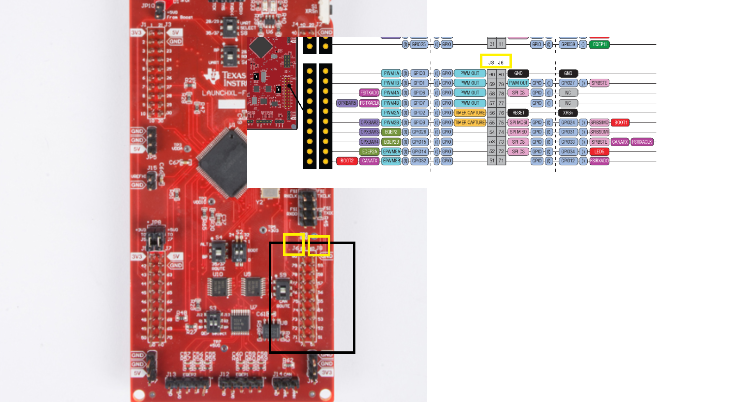
For F280049C LaunchPad I see that the pin order of the LaunchPad does not match with the one mentioned in the specification. In the manual I see that the order of the pins is J8 and J6 from left to right but in the launchPad i see the order as J6 and J8 from left to right. See the picture below. Also when I try to access the pin, I found that the order as per the board J6 and J8 does not work and the order mentioned in the manual is correct. Can you check on this?


  • Aditya,

    Thank you for pointing out this issue. You are correct that there is an inconsistency.

    The outer row on that header should be J6 with pin numbers 51-60. The inner row is J8 with pin numbers 71-80. The pin labels are correct on the bottom side of the board. 

     In http://www.ti.com/lit/SPRUII7, Figure 3the pin numbering is swapped between J6 and J8, though the Signals themselves are in the right location. i.e. GND is the upper right-most pin. 

    In the schematic Sheet 2 (also Figure 5 in SPRUII7), J6 and J8 labels are swapped, but the signals are correct.

    I will be submitting documentation fixes and will correct the schematic for the next revision of the PCB. I cannot tell you when the next revision will be released. 

    Thanks for pointing this out.

    Regards,
    Mark