


Tool/software: Code Composer Studio
Hi, I am using the McBSP feature of the Delfino to generate a SPI style waveform for interfacing with a sensor. The sensor requires a long stream of clocks to read in data serially over a MISO data pin.

I am achieving this functionality by configuring the McBSP peripheral on the Delfino to use 3 frames of 16-bit words, and then using DMA to read in the data from the sensor.
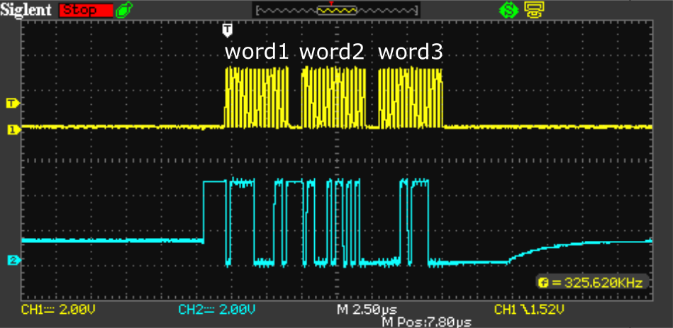
This works well for the most part. Most of the time DMA correctly populates the correct memory locations with the corresponding 3 words. However, my problem is that periodically (1 per 100,000 transactions or so) the words get swapped in memory. After this, DMA continually populates the incorrect memory locations (word1 stored as word2, word2 stored as word3, word3 stored as word1).

I'm currently attempting to detect when this happens and then correcting the problem by resetting the McBSP and DMA peripherals. I would prefer to fix the underlying problem so that it doesn't occur in the first place.
I'm monitoring the following error registers on the two peripherals but none of them show any recorded errors:
McbspbRegs.SPCR1.bit.RFULL
McbspbRegs.SPCR1.bit.RSYNCERR
McbspbRegs.SPCR2.bit.XSYNCERR
DmaRegs.CH3.CONTROL.bit.OVRFLG
DmaRegs.CH4.CONTROL.bit.OVRFLG
Below is the core code that implement the McBSP and DMA transactions.
//DMA memory allocation
// Place sdata2 and rdata2 buffers in DMA-accessible RAM
#pragma DATA_SECTION(sdata2, "DMARAML4")
#pragma DATA_SECTION(rdata2, "DMARAML4")
Uint16 sdata2; // Sent Data sensor 2
Uint16 rdata2; // Received Data sensor 2

//DMA register configuration
EALLOW;
DmaRegs.DMACTRL.bit.HARDRESET = 1;
asm(" NOP");
// Only 1 NOP needed per Design
EDIS;

transData = sdata2;
recvData = rdata2;

EALLOW;
DmaRegs.CH3.MODE.bit.CHINTE = 0;
// Channel 3, McBSPB transmit
DmaRegs.CH3.BURST_SIZE.all = 0; // 1 word/burst
DmaRegs.CH3.SRC_BURST_STEP = 0; // no effect when using 1 word/burst
DmaRegs.CH3.DST_BURST_STEP = 0; // no effect when using 1 word/burst
DmaRegs.CH3.TRANSFER_SIZE = 2; // Interrupt every 3 frames (3 bursts/transfer)
DmaRegs.CH3.SRC_TRANSFER_STEP = 1; // Move to next word in buffer after each word in a burst
DmaRegs.CH3.DST_TRANSFER_STEP = 0; // Don't move destination address
DmaRegs.CH3.SRC_ADDR_SHADOW = (Uint32) sdata2; // Start address = buffer
DmaRegs.CH3.SRC_BEG_ADDR_SHADOW = (Uint32) sdata2; // Not needed unless using wrap function
DmaRegs.CH3.DST_ADDR_SHADOW = (Uint32) &McbspbRegs.DXR1.all; // Start address = McBSPB DXR
DmaRegs.CH3.DST_BEG_ADDR_SHADOW = (Uint32) &McbspbRegs.DXR1.all; // Not needed unless using wrap function
DmaRegs.CH3.CONTROL.bit.PERINTCLR = 1; // Clear peripheral interrupt event flag
DmaRegs.CH3.CONTROL.bit.SYNCCLR = 1; // Clear sync flag
DmaRegs.CH3.CONTROL.bit.ERRCLR = 1; // Clear sync error_novotechnik flag
DmaRegs.CH3.DST_WRAP_SIZE = 0xFFFF; // Put to maximum - don't want destination wrap
DmaRegs.CH3.SRC_WRAP_SIZE = 0xFFFF; // Put to maximum - don't want source wrap
DmaRegs.CH3.MODE.bit.SYNCE = 0; // No sync signal
DmaRegs.CH3.MODE.bit.SYNCSEL = 0; // No sync signal
DmaRegs.CH3.MODE.bit.CHINTE = 1; // Enable channel interrupt
DmaRegs.CH3.MODE.bit.CHINTMODE = 1; // Interrupt at end of transfer
DmaRegs.CH3.MODE.bit.PERINTE = 1; // Enable peripheral interrupt event
DmaRegs.CH3.MODE.bit.PERINTSEL = DMA_MXREVTB; // Peripheral interrupt select = McBSP MXSYNCB
DmaRegs.CH3.MODE.bit.CONTINUOUS = 0; //continuous: (1) DMA re-initializes when TRANSFER_COUNT is zero and waits for the next interrupt event trigger
DmaRegs.CH3.CONTROL.bit.PERINTCLR = 1; // Clear any spurious interrupt flags

// Channel 4, McBSPB Receive
DmaRegs.CH4.MODE.bit.CHINTE = 0;
DmaRegs.CH4.BURST_SIZE.all = 0; // 1 word/burst
DmaRegs.CH4.SRC_BURST_STEP = 0; // no effect when using 1 word/burst
DmaRegs.CH4.DST_BURST_STEP = 0; // no effect when using 1 word/burst
DmaRegs.CH4.TRANSFER_SIZE = 2; // Interrupt every 3 frames (3 bursts/transfer)
DmaRegs.CH4.SRC_TRANSFER_STEP = 0; // Don't move source address
DmaRegs.CH4.DST_TRANSFER_STEP = 1; // Move to next word in buffer after each word in a burst
DmaRegs.CH4.SRC_ADDR_SHADOW = (Uint32) &McbspbRegs.DRR1.all; // Start address = McBSPB DRR
DmaRegs.CH4.SRC_BEG_ADDR_SHADOW = (Uint32) &McbspbRegs.DRR1.all; // Not needed unless using wrap function
DmaRegs.CH4.DST_ADDR_SHADOW = (Uint32) rdata2; // Start address = Receive buffer (for McBSP-B)
DmaRegs.CH4.DST_BEG_ADDR_SHADOW = (Uint32) rdata2; // Not needed unless using wrap function
DmaRegs.CH4.CONTROL.bit.PERINTCLR = 1; // Clear peripheral interrupt event flag
DmaRegs.CH4.CONTROL.bit.SYNCCLR = 1; // Clear sync flag
DmaRegs.CH4.CONTROL.bit.ERRCLR = 1; // Clear sync error_novotechnik flag
DmaRegs.CH4.DST_WRAP_SIZE = 0xFFFF; // Put to maximum - don't want destination wrap
DmaRegs.CH4.SRC_WRAP_SIZE = 0xFFFF; // Put to maximum - don't want source wrap
DmaRegs.CH4.MODE.bit.CHINTE = 1; // Enable channel interrupt
DmaRegs.CH4.MODE.bit.CHINTMODE = 1; // Interrupt at end of transfer
DmaRegs.CH4.MODE.bit.PERINTE = 1; // Enable peripheral interrupt event
DmaRegs.CH4.MODE.bit.PERINTSEL = DMA_MREVTB; // Peripheral interrupt select = McBSP MRSYNCA
DmaRegs.CH4.MODE.bit.CONTINUOUS = 0; //continuous: (1) DMA re-initializes when TRANSFER_COUNT is zero and waits for the next interrupt event trigger
DmaRegs.CH4.CONTROL.bit.PERINTCLR = 1; // Clear any spurious interrupt flags
EDIS;

//McBSP register configuration
// McBSP-B register settings
McbspbRegs.SPCR2.all = 0x0000; // Reset FS generator, sample rate generator & transmitter
McbspbRegs.SPCR1.all = 0x0000; // Reset Receiver, Right justify word, Digital loopback dis.
McbspbRegs.SPCR1.bit.DLB = 0;
McbspbRegs.SPCR1.bit.CLKSTP = 2; // clock stop mode bits (0-1: disabled, 2: clock stop with no clock delay, 3: clock stop with half-cycle delay)

McbspbRegs.PCR.bit.FSXM = 1; //transmit frame synch mode bit (0: external pin, 1: supplied by sample rate generator)
McbspbRegs.PCR.bit.FSRM = 1; //receive frame synch mode bit (0: external pin, 1: supplied by sample rate generator)
McbspbRegs.PCR.bit.CLKXM = 1; //transmit clock mode bit (in stop clock mode: 0: slave in SPI, 1: master in SPI)
McbspbRegs.PCR.bit.CLKRM = 1; //receive clock mode bit (in loopback mode: 0: MCLKR pin in high impedance state, 1: internal MCLKR driven by internal CLKX)
McbspbRegs.PCR.bit.SCLKME = 0; //sample rate generator input clock mode bit, used with CLKSM to select input clock
McbspbRegs.PCR.bit.DX_STAT = 0; //DX pin bit (0: drive DX pin low, 1: drive DX pin high)
McbspbRegs.PCR.bit.DR_STAT = 0; //DR pin status bit (0: DR pin is low, 1: DR pin is high)
McbspbRegs.PCR.bit.FSXP = 1; //transmit frame-synch polarity bit (0: transmit frame-synch pulses are active high, 1: active low)
McbspbRegs.PCR.bit.FSRP = 0; //receive frame-synch polarity bit (0: receive frame-synch pulses are active high, 1: active low)
McbspbRegs.PCR.bit.CLKXP = 0; //transmit clock polarity bit (transmit data sampled on 0: rising, 1: falling edge)
McbspbRegs.PCR.bit.CLKRP = 1; //receive clock polarity bit (transmit data sampled on 0: falling, 1: rising edge)

McbspbRegs.RCR1.bit.RWDLEN1 = 2; // 16-bit word receive
McbspbRegs.RCR1.bit.RFRLEN1 = 0; // 1-frame receptions
McbspbRegs.RCR2.bit.RDATDLY = 1; // FSX setup time 1 in master mode. 0 for slave mode (Receive)
McbspbRegs.RCR2.bit.RFIG = 1;

McbspbRegs.XCR1.bit.XWDLEN1 = 2; // 16-bit word transmit
McbspbRegs.XCR1.bit.XFRLEN1 = 0; // 1-frame tramsmissions
McbspbRegs.XCR2.bit.XDATDLY = 1; // FSX setup time 1 in master mode. 0 for slave mode (Transmit)
McbspbRegs.XCR2.bit.XFIG = 1;

McbspbRegs.SRGR2.all = 0x0000;
McbspbRegs.SRGR2.bit.CLKSM = 1; //sample rate generator input clock mode bit (used with SCLKME bit)
McbspbRegs.SRGR2.bit.FPER = 0; //frame synch period bits for FSG, FPER = 1 CLKG periods
McbspbRegs.SRGR1.bit.FWID = 0; // Frame Width = 1 CLKG period
McbspbRegs.SRGR1.bit.CLKGDV = 17; //divide-down value for CLKG, SPI_CLK_FREQ = LSPCLK / (CLKGDV+1) => 62.5mhz/18=3.47MHz spi clk

McbspbRegs.SPCR2.bit.GRST = 1; // Enable the sample rate generator
delay_loop(); // Wait at least 2 SRG clock cycles
McbspbRegs.SPCR2.bit.XRST = 1; // Release TX from Reset
McbspbRegs.SPCR1.bit.RRST = 1; // Release RX from Reset
McbspbRegs.SPCR2.bit.FRST = 1; // Frame Sync Generator reset


//start a new SPI read
void APS_Sensor::update() {
if(waitingForUpdate) {
return;
}

waitingForUpdate = 1;

if(McbspbRegs.SPCR1.bit.RFULL) {
MCBSP_RFULL_count++; //receive overrun condition, we've lost some data, not seeing any errors here
}
if(McbspbRegs.SPCR1.bit.RSYNCERR) {
MCBSP_RSYNCERR_count++; //not seeing any errors here
}
if(McbspbRegs.SPCR2.bit.XSYNCERR) {
MCBSP_XSYNCERR_count++; //not seeing any errors here
}

EALLOW;
if(DmaRegs.CH3.CONTROL.bit.OVRFLG) {
DMA1_OVRFLG_count++; //not seeing any errors here
}
if(DmaRegs.CH4.CONTROL.bit.OVRFLG) {
DMA2_OVRFLG_count++;  //not seeing any errors here
}
EDIS;
start_dma(); //start new SPI transaction
}

void APS_Sensor::start_dma(void) {

GpioDataRegs.GPACLEAR.bit.GPIO15 = 1; //activate SS
EALLOW;
DmaRegs.CH3.CONTROL.bit.RUN = 1; // Start DMA Transmit from McBSP-B
DmaRegs.CH4.CONTROL.bit.RUN = 1; // Start DMA Receive from McBSP-B
EDIS;
}

// INT7.3
__interrupt void local_D_INTCH3_ISR(void) // DMA Ch3 (transmit)
{

EALLOW;
DmaRegs.CH3.CONTROL.bit.RUN = 0; // Re-enable DMA CH1. Should be done every transfer
EDIS;

PieCtrlRegs.PIEACK.all = PIEACK_GROUP7; // To receive more interrupts from this PIE group, acknowledge this interrupt

return;
}

// INT7.4
__interrupt void local_D_INTCH4_ISR(void) // DMA Ch4 (receive)
{
OutputAPS->newDataReceived();

EALLOW;
DmaRegs.CH4.CONTROL.bit.RUN = 0; // Re-enable DMA CH2. Should be done every transfer
EDIS;

PieCtrlRegs.PIEACK.all = PIEACK_GROUP7; // To receive more interrupts from this PIE group, acknowledge this interrupt

return;
}

Uint16 LA11_APS_Sensor::newDataReceived(void) {

LA11_26_APS_output.words.word1 = recvData[0];
LA11_26_APS_output.words.word2 = recvData[1];
LA11_26_APS_output.words.word3 = recvData[2];

nextSampleTime = addTime_uS(getCurrentTime(), LA11_FRAME_SPACING_US);

GpioDataRegs.GPASET.bit.GPIO15 = 1; //deactivate SS

waitingForUpdate = 0;

return 0;
}
Any suggestions on how to fix or further debug this problem would be appreciated. Thanks.


