This thread has been locked.

If you have a related question, please click the "Ask a related question" button in the top right corner. The newly created question will be automatically linked to this question.

F28M36P63C2: Cannot write odd memory in EPI SDRAM memory

Part Number: F28M36P63C2
Other Parts Discussed in Thread: TMDSHSECDOCK

Dear Sirs,

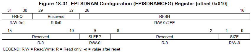
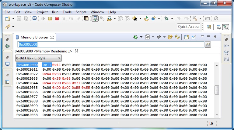
We have added SDRAM to the EPI as per the Table 18-1 of the SPRUHE8D.pdf data sheet. The SDRAM chip is we used is a IS42S16800F 128Mbit (8M x 16). We placed this at a base address of 0x60000000. We used the SDRAM software example in the Control Suite. It works fine for even addresses when accessing 16 bit and 32 bit data sizes. However, we cannot write 8 bit data at odd addresses. Below is a debug output example of our problem:

Wrote 0 to address 60002000
Wrote 1 to address 60002001
Wrote 2 to address 60002002
Writing 3 to address 60002003
Read 0 from address 60002000
Read 0 from address 60002001
Read 2 from address 60002002
Read 2 from address 60002003

Thank your for your help.
  • Drew,

    Did you update the EPISDRAMCFG register to match your SDRAM configuration?

    -Tommy

  • Below are our settings, it is based on your example in epi_sdram.c. The only change is with the size of the SDRAM as noted:

        // Set clock divider to 1 (divide by 2)
        EPIDividerSet(EPI0_BASE, 1);

        // Enable SDRAM mode
        EPIModeSet(EPI0_BASE, EPI_MODE_SDRAM);

        // System clock frq between 50-100MHz
        // Sleep mode disabled.
        // Refresh Count = 0x2EE (default value)

        EPIConfigSDRAMSet(EPI0_BASE, (EPI_SDRAM_CORE_FREQ_50_100 | EPI_SDRAM_FULL_POWER | EPI_SDRAM_SIZE_128MBIT), 750);  // Was 512 MBIT ours is 128MBIT

        // External RAM Size (to set proper address range) 256MB
        // External RAM Address = 0x60000000
        EPIAddressMapSet(EPI0_BASE, (EPI_ADDR_RAM_SIZE_16MB | EPI_ADDR_RAM_BASE_6));  // Was 256MB, ours is 16MB

  • Drew,

    That looks ok to me.

    Can you open a Memory Browser and poke at the SDRAM contents manually to see if you are able to update bytes?

    Also try to modify the memory contents through the Expressions window using the dereferenced pointer address: *(char *)0x60000001

    If the above two access methods work, then it likely has something to do with the code/compiler.

    -Tommy

  • Hi Tommy,

    We ran the test you suggested and it worked correctly. That is we could write a byte using the expression window and read the memory area back using the memory browser. There was no overwriting of bytes. In fact when we use the C function to read from SDRAM, the data is read back correctly.

    So it appears the problem is writing a byte to the SDRAM using the compiled code. This is only a problem with the SDRAM area. When we use the chip's on board RAM, we can write and read bytes correctly.

    What do we do now?

    Thanks again.

  • Drew,

    Any pointer accesses that work in the Expressions window should also work in your code so you can try that in your program.

    If you have to use data structures, please share the code snippet that is used to write the data. Include the declarations of variables that are used for referencing the memory (for example if you have declared an array in SDRAM space).

    If there is nothing obvious with the code snippet, we may need to look at the compiler-generated assembly to see if incorrect instructions are created.

    -Tommy
  • Hi Tommy,

    We have been using pointer access to test the SDRAM all along. Below is a snippet of our code:

    unsigned long lAddr;

    char *addressC;
    long value;

            addressC = (char *)lAddr;
            *addressC = (char)value;

    We can set the value of lAddr and value over the serial interface. This works perfectly for processor onboard RAM. I have isolated the associated assembly language instructions that the compiler produces for the above code:

        .dwpsn    file "../CmdMgr.c",line 729,column 9,is_stmt,isa 1
            LDR       A2, [SP, #16]         ; [DPU_V7M3_PIPE] |729|
            LDRB      A1, [SP, #28]         ; [DPU_V7M3_PIPE] |729|
            STRB      A1, [A2, #0]          ; [DPU_V7M3_PIPE] |729|

    I have used the debugger to view the registers while executing this instructions and they are as expected. Byte access does work correctly using the expression and memory browser.

    Are there any settings in the EPI,or the processor, that handles byte order or that may affect this condition in any way? Our goal is to run code out of the SDRAM so this needs to work I would imagine.

    We are stumped.

  • Hi Tommy,

    We have two prototype boards that exhibit the same problem. We can send you one for you to test if that would help solve this problem. Please let us know what we can do.

    Thanks

    Drew

  • Drew,

    I apologize for missing your reply on Thursday.

    Is my understanding correct that you are able to see correct byte access when stepping through the assembly code?

    If that is the case, it may be worth trying to slow down your system speed to see if there is a timing issue that is corrupting the SDRAM instructions. For example, set the PLL output to half of your normal operating speed.

    -Tommy
  • You may need to adjust the EPISDRAMCFG[RFSH] value as well to scale with the slower frequency.
  • Hi Tommy,

    We slowed the SDRAM clock to 12.5 Mhz and the problem still persists. Below are the details:

    The original configuration was 37.5 MHz.

     Original Settings…

     400D0008 = 0

    400D0004 = 1

     We slowed it down to 12.5 MHz. (Verified with Oscope)

     New Settings…

     400D0008 = 0

    400D0004 = 4

     The refresh was recalculated…

     (64000/8192) 0.08 = 97.6

     Used Decimal 90 = 5A

     400D0010 changed to 5A0001

    No change in behavior.

     What can we do next?

  • Is there a specific SDRAM chip that you recommend using that has been tested? We can change our chip if needed.

  • Drew,

    Based on your observations, I am inclined to believe that the SDRAM and EPI interface are working properly.  It sounds as though memory access works when you interactively execute code through a debug connection, but not when you let the application run freely.  Is that correct?

    Your question regarding order of execution prompted me to look in the TRM for M3 integration details where I found this:

    It looks like the EPI memory space at 0x60000000 is Normal memory where transactions can be re-ordered.

    This might explain your observations where interactive (slow) execution of code may prevent re-ordering because the pipeline can flush between instructions, but free-running (fast) execution allows the re-ordering to take place.  (I do not know for sure if the pipeline flushes at breakpoints)

    You might try to change the pointer from char to volatile char to see if the compiler will automatically generate Barrier instructions to preserve transaction order.

    -Tommy

  • Hi Tommy,

    We changed the (pointer to a char) to a (pointer to a volatile char) and it did not make any difference. I checked the assembly code that the compiler created and it was exactly the same as with a pointer to a char. We did some more testing with different conditions and it is not just that we can not write to odd locations for bytes. There are other conditions that cause problems. A single byte write to an even address causes the next higher odd address to get a duplicate of the even address value.

    Below is an illustration of the six cases we see writing to SDRAM. These results are very repeatable. Only two cases are correct when running the application. Using the Memory Browser and Expression Window it all works as we would expect.

    Case 1: Single byte write to an even address.

    Command: wr 1 60002000 11

    Result: The correct byte is written with the data, but the next higher byte is written, also.

     Case 2: Single byte write to an odd address.

    Command: wr 1 60002011 22

    Result: No data is written.

     Case 3: Two byte write to an even address.

    Command: wr 2 60002022 3344

    Result: Works Correctly.

     Case 4: Two byte write to an odd address.

    Command: wr 2 60002033 5566

    Result: The Second Byte is correct, but the first byte is at the address higher than the second, not the location lower.

     Case 5: Four byte write to an even address.

    Command: wr 4 60002044 778899AA

    Result: Works Correctly.

     Case 6: Four byte write to an odd address.

    Command: wr 4 60002055 BBCCDDEE

    Result: As with the two byte write, the lowest byte is placed at the wrong end, one address higher than the highest correct byte.

     Below is the memory window after the above was executed. All of the locations were initialized to 0 before starting.


    We also did a test of memory location 2002f664. This is in the processor RAM and byte write does work correctly.

    >RD long 6e616353 from address 2002f664

    >WR byte aa to address 2002f664

    >RD long 6e6163aa from address 2002f664  (ONLY THE AA CHANGED)

    What is our next step?

    Drew

  • Drew,

    Thanks for the additional results. That seems to be pointing another direction now.

    Would you be able to share the EPI -> SDRAM schematics and the EPI register settings?

    I usually do a ground-up verification of signal mapping and register values when I'm out of ideas.

    -Tommy
  • Hi Tommy,

    We don't have a schematic but we do have a wire list / assignment, see below:

    IS42S16800 BOTTOM VIEW
    PIN           PIN
    GND -------- 54 VSS   VDD 1 -------- 3V3
    123 -------- 53 DQ15 DQ0 2 -------- 105
    GND -------- 52 VSSQ VDDQ 3 -------- 3V3
    91 -------- 51 DQ14 DQ1 4 -------- 103
    89 -------- 50 DQ13 DQ2 5 -------- 133
    3V3 -------- 49 VDDQ VSSQ 6 -------- GND
    122 -------- 48 DQ12 DQ3 7 -------- 134
    109 -------- 47 DQ11 DQ4 8 -------- 137
    GND -------- 46 VSSQ VDDQ 9 -------- 3V3
    107 -------- 45 DQ10 DQ5 10 -------- 138
    77 -------- 44 DQ9 DQ6 11 -------- 99
    3V3 -------- 43 VDDQ VSSQ 12 -------- GND
    75 -------- 42 DQ8 DQ7 13 -------- 101
    GND -------- 41 VSS VDD 14 -------- 3V3
      -------- 40 NC DQML 15 -------- 104
    106 -------- 39 DQMH WE 16 -------- 125
    96 -------- 38 CLK CAS 17 -------- 108
    127 -------- 37 CKE RAS 18 -------- 110
    122 -------- 36 NC CS 19 -------- 126
    109 -------- 35 A11 BA0 20 -------- 89
    77 -------- 34 A9 BA1 21 -------- 91
    75 -------- 33 A8 A10 22 -------- 107
    101 -------- 32 A7 A0 23 -------- 105
    99 -------- 31 A6 A1 24 -------- 103
    138 -------- 30 A5 A2 25 -------- 133
    137 -------- 29 A4 A3 26 -------- 134
    GND -------- 28 VSS   VDD 27 -------- 3V3
             

    The register settings are pretty much from your SDRAM example. Below is the code from init_sdram() and SetPortControl() from the file epi_sdram.c:

    //*****************************************************************************
    //
    // This is pin mux configuration function to bring the EPI signals on required
    // ports of device.
    //
    //*****************************************************************************

    void SetPortControl(void)  {
        //
        // GPIO Port C pins
        //

        HWREG(GPIO_PORTC_BASE + GPIO_O_PCTL) = GPIO_PCTL_PC4_EPI0S2 |
                                               GPIO_PCTL_PC5_EPI0S3 |
                                               GPIO_PCTL_PC6_EPI0S4 |
                                               GPIO_PCTL_PC7_EPI0S5;

        //
        // GPIO Port E pins
        //
        HWREG(GPIO_PORTE_BASE + GPIO_O_PCTL) = GPIO_PCTL_PE0_EPI0S8 |
                                               GPIO_PCTL_PE1_EPI0S9;

        //
        // GPIO Port F pins
        //

        HWREG(GPIO_PORTF_BASE + GPIO_O_PCTL) = GPIO_PCTL_PF4_EPI0S12 |
                                               GPIO_PCTL_PF5_EPI0S15;
        //
        // GPIO Port G pins
        //
        HWREG(GPIO_PORTG_BASE + GPIO_O_PCTL) = GPIO_PCTL_PG0_EPI0S13 |
                                               GPIO_PCTL_PG1_EPI0S14 |
                                               GPIO_PCTL_PG7_EPI0S31;
        //
        // GPIO Port H pins
        //
        HWREG(GPIO_PORTH_BASE + GPIO_O_PCTL) = GPIO_PCTL_PH0_EPI0S6 |
                                               GPIO_PCTL_PH1_EPI0S7 |
                                               GPIO_PCTL_PH2_EPI0S1 |
                                               GPIO_PCTL_PH3_EPI0S0 |
                                               GPIO_PCTL_PH4_EPI0S10 |
                                               GPIO_PCTL_PH5_EPI0S11;
        //
        // GPIO Port J pins
        //
        HWREG(GPIO_PORTJ_BASE + GPIO_O_PCTL) = GPIO_PCTL_PJ0_EPI0S16 |
                                               GPIO_PCTL_PJ1_EPI0S17 |
                                               GPIO_PCTL_PJ2_EPI0S18 |
                                               GPIO_PCTL_PJ3_EPI0S19 |
                                               GPIO_PCTL_PJ4_EPI0S28 |
                                               GPIO_PCTL_PJ5_EPI0S29 |
                                               GPIO_PCTL_PJ6_EPI0S30;
    }

    //*****************************************************************************
    //
    // init_sdram
    //
    //*****************************************************************************
    void init_sdram(Io *io) {

        // Disable Protection
        HWREG(SYSCTL_MWRALLOW) =  0xA5A5A5A5;

        // Setup main clock tree for 75MHz - M3 and 150MHz - C28x
        SysCtlClockConfigSet(SYSCTL_SYSDIV_1 | SYSCTL_M3SSDIV_2 | SYSCTL_USE_PLL |
                             (SYSCTL_SPLLIMULT_M & 0x0F));

        // Enable Clock for EPI & GPIO Ports
        SysCtlPeripheralEnable(SYSCTL_PERIPH_EPI0);

        SysCtlPeripheralEnable(SYSCTL_PERIPH_GPIOC);
        SysCtlPeripheralEnable(SYSCTL_PERIPH_GPIOE);
        SysCtlPeripheralEnable(SYSCTL_PERIPH_GPIOF);
        SysCtlPeripheralEnable(SYSCTL_PERIPH_GPIOG);
        SysCtlPeripheralEnable(SYSCTL_PERIPH_GPIOH);
        SysCtlPeripheralEnable(SYSCTL_PERIPH_GPIOJ);

        // Configure the GPIO setting for the EPI pins.
        SetPortControl();

        GPIODirModeSet(GPIO_PORTC_BASE,
                       (GPIO_PIN_4 | GPIO_PIN_5 | GPIO_PIN_6 | GPIO_PIN_7),
                       GPIO_DIR_MODE_HW);

        GPIOPadConfigSet(GPIO_PORTC_BASE,
                         (GPIO_PIN_4 | GPIO_PIN_5 | GPIO_PIN_6 | GPIO_PIN_7),
                         GPIO_PIN_TYPE_STD_WPU);

        GPIODirModeSet(GPIO_PORTE_BASE,
                       (GPIO_PIN_0 | GPIO_PIN_1),
                       GPIO_DIR_MODE_HW);

        GPIOPadConfigSet(GPIO_PORTE_BASE,
                         (GPIO_PIN_0 | GPIO_PIN_1 | GPIO_PIN_2 | GPIO_PIN_3),
                         GPIO_PIN_TYPE_STD_WPU);

        GPIODirModeSet(GPIO_PORTF_BASE,
                       (GPIO_PIN_4 | GPIO_PIN_5),
                       GPIO_DIR_MODE_HW);

        GPIOPadConfigSet(GPIO_PORTF_BASE,
                         (GPIO_PIN_4 | GPIO_PIN_5),
                         GPIO_PIN_TYPE_STD_WPU);

        GPIODirModeSet(GPIO_PORTG_BASE,
                       (GPIO_PIN_0 | GPIO_PIN_1),
                       GPIO_DIR_MODE_HW);

        GPIOPadConfigSet(GPIO_PORTG_BASE,
                         (GPIO_PIN_0 | GPIO_PIN_1),
                         GPIO_PIN_TYPE_STD_WPU);

        GPIODirModeSet(GPIO_PORTG_BASE,
                       GPIO_PIN_7,
                       GPIO_DIR_MODE_HW);

        GPIOPadConfigSet(GPIO_PORTG_BASE,
                         GPIO_PIN_7,
                         GPIO_PIN_TYPE_STD_WPU);

        GPIODirModeSet(GPIO_PORTH_BASE,
                       (GPIO_PIN_0 | GPIO_PIN_1 | GPIO_PIN_2 | GPIO_PIN_3 |
                       GPIO_PIN_4 | GPIO_PIN_5),
                       GPIO_DIR_MODE_HW);

        GPIOPadConfigSet(GPIO_PORTH_BASE,
                         (GPIO_PIN_0 | GPIO_PIN_1 | GPIO_PIN_2 | GPIO_PIN_3 |
                         GPIO_PIN_4 | GPIO_PIN_5),
                         GPIO_PIN_TYPE_STD_WPU);

        GPIODirModeSet(GPIO_PORTJ_BASE,
                       (GPIO_PIN_0 | GPIO_PIN_1 | GPIO_PIN_2 | GPIO_PIN_3 |
                       GPIO_PIN_4 | GPIO_PIN_5 | GPIO_PIN_6),
                       GPIO_DIR_MODE_HW);

        GPIOPadConfigSet(GPIO_PORTJ_BASE,
                         (GPIO_PIN_0 | GPIO_PIN_1 | GPIO_PIN_2 | GPIO_PIN_3 |
                         GPIO_PIN_4 | GPIO_PIN_5 | GPIO_PIN_6),
                         GPIO_PIN_TYPE_STD_WPU);

        // Set clock divider to 1 (divide by 2)
        EPIDividerSet(EPI0_BASE, 1);

        // Enable SDRAM mode
        EPIModeSet(EPI0_BASE, EPI_MODE_SDRAM);

        // System clock frq between 50-100MHz
        // Sleep mode disabled.
        // Refresh Count = 0x2EE (default value)

    // NOTE WE TRIED BOTH OF THE FOLLOWING LINES, NEITHER WORKED
    //    EPIConfigSDRAMSet(EPI0_BASE, (EPI_SDRAM_CORE_FREQ_50_100 | EPI_SDRAM_FULL_POWER | EPI_SDRAM_SIZE_512MBIT), 750);
        EPIConfigSDRAMSet(EPI0_BASE, (EPI_SDRAM_CORE_FREQ_50_100 | EPI_SDRAM_FULL_POWER | EPI_SDRAM_SIZE_128MBIT), 750);

        // External RAM Size (to set proper address range) 256MB
        // External RAM Address = 0x60000000

    // NOTE WE TRIED BOTH OF THE FOLLOWING LINES, NEITHER WORKED
        EPIAddressMapSet(EPI0_BASE, (EPI_ADDR_RAM_SIZE_256MB | EPI_ADDR_RAM_BASE_6));
    //    EPIAddressMapSet(EPI0_BASE, (EPI_ADDR_RAM_SIZE_16MB | EPI_ADDR_RAM_BASE_6));

        // Wait for EPI SDRAM init sequence to complete
        while(HWREG(EPI0_BASE + EPI_O_STAT) & EPI_STAT_INITSEQ)
        {
        }
    }

    Thanks,

    Drew

  • It looks the image for the memory browser did not post correctly. Here is the screen capture for the post for a few days ago.

  • Drew,

    It looks like you are connecting the SDRAM to a controlCARD.  Is that correct?  Is the SDRAM installed on a custom board with a dock header?

    When you write 2- and 4-bytes to SDRAM, are you using consecutive *char pointer writes or are you using *short and *int pointers?

    -Tommy

  • Hi Tommy,

    Yes we have connected the SDRAM to a F28M36 control card using the TMDSHSECDOCK card. The SDRAM is installed on an adapter board and the adapter board is installed on the dock header. Below is the link to the adapter board: 

    We are using pointers to short and pointer to long (* short) and (* long). We only use pointer to char for one byte writes (* byte). That's how we tested in the expression window.

    Thanks,

    Drew

  • Drew,

    Given the setup description, I suspect that poor signal integrity and/or propagation delay might be contributing to the flaky behavior. The SDRAM signals are having to travel through multiple transitions between endpoints. Further, the path from the HSEC header to the prototype vias and through the Chip Quick adapter are probably not length matched.

    I would recommend running a malfunctioning memory write loop and scoping the command signals relative to the SDRAM CLK at the physical pins of the SDRAM memory. It may be possible to identify the culprit this way.

    Another option would be to use EPI with an asynchronous SRAM memory where the timing relationships are more forgiving.

    -Tommy
  • Hi Tommy,

    We were concerned about the timing and that is why we kept the clock slow. We tried it at 12.5Mhz, per your request, with the same results.

    We have never yet got a failure when writing and reading words or half words, only with bytes and non-word-aligned words. This error condition is very, very repeatable. If it were clock timing I would expect problems and errors when writing words as well and unpredictable results. This error is very, very repeatable and predictable. For instance when writing a byte to an even location that exact byte will be duplicated in the next higher byte location. The behavior is not flaky it is very predictable. 

    We have a huge constraint on space in our product. That is one reason we liked the EPI SDRAM controller and the SDRAM chip.

    What SDRAM chip or chip set did you use to test the EPI SDRAM interface? We are not tied to this SDRAM chip, we are happy to try others.

    Thanks,

    Drew

  • Drew,

    I am confident that this or any other standard SDRAM would work on a custom board where the memory is placed close to the MCU with good routing. I will ask about which SDRAM was used, but the answer may be slow as this was done a number of years ago.

    I understand that the fail behavior is repeatable, but this by itself does not rule out signal integrity issues. Confirming the signal quality and timings using a scope would probably be the most conclusive approach. Another experiment would be to see if the behavior changes when another SDRAM device is used, or even if the behavior changes with temperature. Any shift in behavior would suggest setup problems.

    -Tommy
  • Hi Tommy,

    We do have two complete board assemblies that behave exactly the same. It is a scary leap of faith to design a board that uses this SDRAM while not having it work correctly in a prototype. However you are confident, and we have no other answer at this time. We do have a logic analyzer and Chris and I discussed instrumenting this board if necessary. We can also order a different SDRAM chip.

    Chris is gone for today. He is the hardware side of our team. I will talk to him tonight and get back with you with our next step. We would like your blessing on what ever we decide so we don't go off in a useless direction as this project is getting critical and our schedule is running out.

    Thank you once again.

    Drew

  • Drew,

    I just received word that the EPI SDRAM mode was validated using MT48LC32M16A2.

    -Tommy
  • Excellent. Thanks again Tommy.
  • Hi Tommy,

    Well it looks like this is an "eat crow" message from us. Deep sigh here. We found that both of the prototype boards that we had made had the same wiring error that was causing the strange behavior. We had it corrected and now both boards work correctly.

    It is peculiar that the debugger expression and memory browser had worked and the code did not. Before we discovered the wiring error we had put a logic analyzer on the board. There was a distinct difference between a character write using the debugger and a character write with the code. It was actually hooking up the logic analyzer that allowed us to find the wiring error.

    We appreciate all the time and effort you put in to to help us and I apologize for using up your time.

    TI has always been great at helping us in the past and we thank you for that.

    Of course you may close this issue.

    Thanks so much!

    Drew

  • Drew,

    I'm glad you were able to find the root cause and appreciate your follow up report. It's good to have closure on this issue. Definitely a tricky one to debug!

    We typically consider the CCS expressions and memory browser widgets to be intrusive when debugging external memory activity because the data refresh operations can be erratic. You might have more consistent behavior if you remove all extraneous variables and memory addresses when poking through the debugger.

    -Tommy