


Dear team,
I am trying to use the DCSM in F28377s based on blinky_with_DCSM project. And I followed the below steps:
1. To modify location of linkpointer to 0x50
.sect "dcsm_otp_z1_linkpointer"
.long 0x1FFFFFF8 ;Z1-LINKPOINTER1
.long 0xFFFFFFFF ;Reserved
.long 0x1FFFFFF8 ;Z1-LINKPOINTER2
.long 0xFFFFFFFF ;Reserved
.long 0x1FFFFFF8 ;Z1-LINKPOINTER3
.long 0xFFFFFFFF ;Reserved
2. Allocate Flash B (code location)to Zone 1
.sect "dcsm_zsel_z1"
.long 0xFFFFFFFF ;Z1-EXEONLYRAM
.long 0xFFFFFFFF ;Z1-EXEONLYSECT
.long 0xFFFFFFFF ;Z1-GRABRAM
.long 0xFFFFFFFB ;Z1-GRABSECT
The value of DCSMZ1Regs is shown as below:

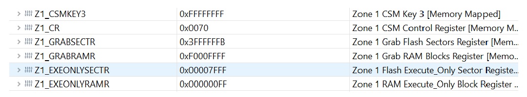 I believe I have done the first 2 steps successfully.
However, when I try to write the CSMPSWDx with the following value:
.long 0x11223344 ;Z1-CSMPSWD0 (LSW of 128-bit password)
.long 0xFFFFFFFF ;Z1-CSMPSWD1
.long 0xFFFFFFFF ;Z1-CSMPSWD2
.long 0xFFFFFFFF ;Z1-CSMPSWD3 (MSW of 128-bit password)
The error occurs:
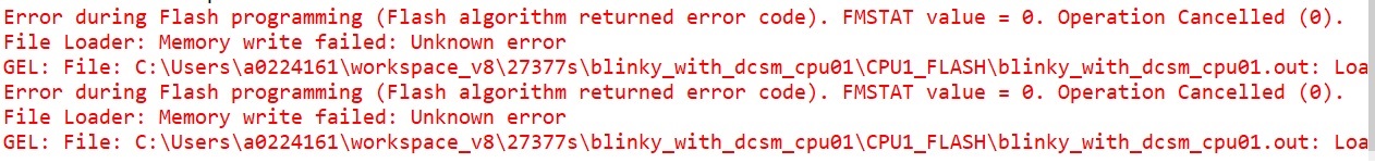
If I change value back to all F, the code can be load without error.
In the memory browser, I could observe the value in CSMPSWDx is "all F". So the value of 11223344 should be able to be written.

Does the ECC decides the value in Zonex OTP Flash must follow certain order?
Thanks for your help.


