


Other Parts Discussed in Thread: TMS320F28032
Hi
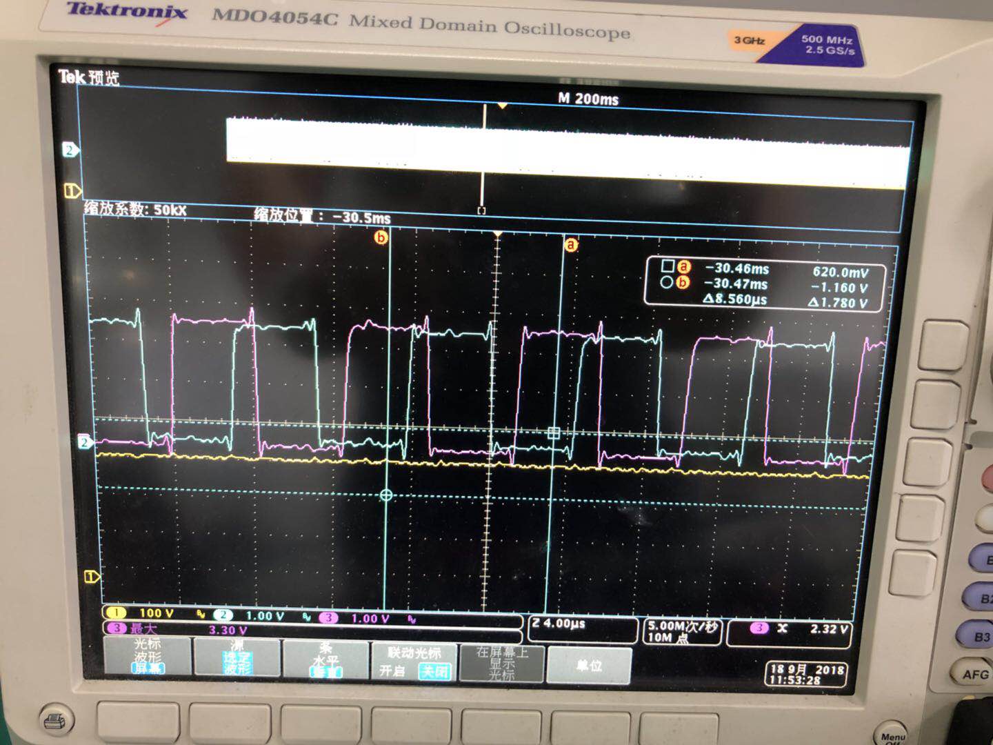
ePWM1A and ePWM2A are configured as driver signal of LLC circuit. So the driver signal should be interleaved.But the driver signal sent from DSP is overlapping sometimes.ePWM1A is configured as hight bridge driver and ePWM2A is configured as low bridge driver. PWM1 TZ1 int is configured as OCP. When OCP event occurs, the driver signal of PWM1A and PWM2A are forced to low, then it will restart .After about 20 times
of OCP,when it restarts, the driver signal is disorder.
//#########################################################
//
// FILE:   DSP280x_EPwm.c
//
// TITLE:  DSP280x ePWM Initialization & Support Functions.
//
//#########################################################
// Running on TMS320LF280xA
// External clock is 20MHz, PLL * 10/2 , CPU-Clock 100 MHz
// Date: from 2005/12/28      , jurgen lv
// Version:1.00     Change Date:
//#########################################################

#include "DSP280x_Device.h"     // DSP280x Headerfile Include File

//---------------------------------------------------------------------------
// InitEPwm:
//---------------------------------------------------------------------------
// This function initializes the ePWM(s) to a known state.
//
void InitEPwm(void)
{
	// Initialize ePWM1/2/3

	InitEPwm1Gpio();
	InitEPwm2Gpio();
//	InitEPwm3Gpio();
	InitEPwm5Gpio();


//	InitTzGpio();

	EALLOW;
	EPwm1Regs.AQSFRC.bit.RLDCSF = 0x00;		// DCDC-DRA
	EPwm2Regs.AQSFRC.bit.RLDCSF = 0x00;		// DCDC-DRB
	EPwm5Regs.AQSFRC.bit.RLDCSF = 0x03;		// for PFC


	EPwm1Regs.AQCSFRC.all = 0x05;		//PWM1A,PWM1B force low
	EPwm2Regs.AQCSFRC.all = 0x05;		//PWM2A,PWM2B force low�
	EPwm5Regs.AQCSFRC.all = 0x05;		//PWM3A,PWM3B force low


	SysCtrlRegs.PCLKCR0.bit.TBCLKSYNC = 0;      // Stop all the TB clocks


/*DC AND PFC OCP TZ initial*/
	////  COMP1A FOR DCOCP  TZ2 FOR DCOCP EVT1 FOR OSHT
// no use TZ module

   	EPwm1Regs.DCTRIPSEL.bit.DCAHCOMPSEL = DC_COMP3OUT;        // DCAH = COMP1OUT
   	EPwm1Regs.DCTRIPSEL.bit.DCALCOMPSEL = DC_TZ2;        // DCAL = TZ2
   	EPwm1Regs.TZDCSEL.bit.DCAEVT1 = TZ_DCAH_HI; // DCAEVT1 =  DCAH high, DCAL do not care;
   	EPwm1Regs.DCACTL.bit.EVT1SRCSEL = DC_EVT1;           // DCAEVT1 = DCAEVT1 (not filtered)
   	EPwm1Regs.DCACTL.bit.EVT1FRCSYNCSEL = DC_EVT_ASYNC;  // Take async path

   	EPwm1Regs.TZSEL.bit.DCAEVT1 = 1; //Enable DCAEVT1 as one-shot-trip source for this ePWM module.
   	EPwm1Regs.TZCTL.bit.TZA = TZ_FORCE_LO;           // EPWM1A will go low

   	// for DCDC ocp
//	EPwm1Regs.TZSEL.bit.OSHT2 = TZ_ENABLE;	//DCAEVT1�������� OSHT ����TZ2��
//	EPwm1Regs.TZCTL.bit.TZA = TZ_FORCE_LO;
	EPwm1Regs.TZCLR.all = 0x0007; //clear all TZFLAG
	EPwm1Regs.TZEINT.bit.OST = 1;	//enable interrupt


   //////  COMP1A FOR DCOCP  TZ2 FOR DCOCP EVT1 FOR OSHT
   // Define an event (DCAEVT2) based on COMP1OUT
/*
   	EPwm2Regs.DCTRIPSEL.bit.DCAHCOMPSEL = DC_COMP3OUT;        // DCAH = COMP1OUT
   	EPwm2Regs.DCTRIPSEL.bit.DCALCOMPSEL = DC_TZ2;        // DCAL = TZ2
   	EPwm2Regs.TZDCSEL.bit.DCAEVT1 = TZ_DCAH_HI; // DCAEVT1 =  DCAH high, DCAL do not care;
   	EPwm2Regs.DCACTL.bit.EVT1SRCSEL = DC_EVT1;           // DCAEVT1 = DCAEVT1 (not filtered)
   	EPwm2Regs.DCACTL.bit.EVT1FRCSYNCSEL = DC_EVT_ASYNC;  // Take async path

   	EPwm2Regs.TZSEL.bit.DCAEVT1 = 1; //Enable DCAEVT1 as one-shot-trip source for this ePWM module.
   	EPwm2Regs.TZCTL.bit.TZA = TZ_FORCE_LO;           // EPWM1A will go low


 //  	EPwm2Regs.TZSEL.bit.OSHT2 = TZ_ENABLE;	//DCAEVT1�������� OSHT ����TZ2��
//	EPwm2Regs.TZCTL.bit.TZA = TZ_FORCE_LO;
	EPwm2Regs.TZEINT.bit.OST = 0;	//disable interrupt

*/


/*
   //EPWM3 DZ PFCOCP COMP2A TZ1
   ////  COMP2A FOR DCOCP  TZ1 FOR DCOCP EVT2 FOR CBC

   EPwm3Regs.DCTRIPSEL.bit.DCAHCOMPSEL = DC_COMP2OUT;        // DCAH = COMP2OUT
   EPwm3Regs.DCTRIPSEL.bit.DCALCOMPSEL = DC_TZ1;        // DCAL = TZ1
   EPwm3Regs.TZDCSEL.bit.DCAEVT2 = TZ_DCAH_HI; // DCAEVT2 =  DCAH high, DCAL do not care;
   EPwm3Regs.DCACTL.bit.EVT2SRCSEL = DC_EVT2;           // DCAEVT2 = DCAEVT2 (not filtered)
   EPwm3Regs.DCACTL.bit.EVT2FRCSYNCSEL = DC_EVT_ASYNC;  // Take async path

   // Enable DCAEVT2 as a cycle-by-cycle trip source
   // Note: DCxEVT1 events can be defined as one-shot.
   //       DCxEVT2 events can be defined as cycle-by-cycle.
   EPwm3Regs.TZSEL.bit.DCAEVT2 = 1;   //Enable DCAEVT2 as CBC-trip source for this ePWM module.


   EPwm3Regs.TZCTL.bit.TZA = TZ_FORCE_LO;           // EPWM2A will go high
   //EPwm1Regs.TZCTL.bit.TZB = TZ_FORCE_LO;           // EPWM2B will go low

    // Enable TZ interrupt
   EPwm3Regs.TZEINT.bit.CBC = 0;//Disable CBC interrupt generation

	// for pfc ocp
//	EPwm3Regs.TZSEL.bit.CBC1 = TZ_ENABLE;  //Enable DCAEVT2 as CBC-trip source for this ePWM module.
//	EPwm3Regs.TZCTL.bit.TZA = TZ_FORCE_LO;
//	EPwm3Regs.TZEINT.bit.CBC = 0;	//disable interrupt

*/

	// EPWM1 config for DCDC_DRA  �Ϲ�
	EPwm1Regs.TBPRD = DC_PRD_300K;			//
	EPwm1Regs.TBPHS.half.TBPHS = 0;
	EPwm1Regs.TBCTL.bit.PHSEN = TB_DISABLE;
	EPwm1Regs.TBCTL.bit.SYNCOSEL = TB_CTR_ZERO;		// Pass through
	EPwm1Regs.TBCTL.bit.CTRMODE = TB_COUNT_UPDOWN;	// up/down Count
	EPwm1Regs.TBCTL.bit.PRDLD = TB_SHADOW;//TBPRD is loaded from its shadow register on Counter = 0 event (CTR_zero)
	//TBCLK=SYSCLKOUT/(HSPCLKDIV * CLKDIV)=SYSCLKOUT
	EPwm1Regs.TBCTL.bit.CLKDIV = TB_DIV1;				//Timebase clock pre-scale
	EPwm1Regs.TBCTL.bit.HSPCLKDIV = TB_DIV1;			//High speed time pre-scale
 //   	EPwm1Regs.TBCTL.bit.PHSDIR = TB_UP;		//Phase Direction Down

	////for DCDC pwm compare vlaue
	EPwm1Regs.CMPA.half.CMPA = DC_DUTY_MIN;		// DC_DUTY_MIN=1
	EPwm1Regs.CMPCTL.bit.LOADAMODE =  CC_CTR_ZERO;            // CC_CTR_ZERO_PRD;
	EPwm1Regs.CMPCTL.bit.SHDWAMODE = CC_SHADOW;

	//for DCDC pwm high_low level
	EPwm1Regs.AQCTLA.bit.CAU = AQ_CLEAR;
	EPwm1Regs.AQCTLA.bit.CAD = AQ_SET;

	//ʹ���ֶ���ӵ���������ʹ���Զ����õ�����
	EPwm1Regs.DBCTL.bit.OUT_MODE = DB_DISABLE;
    //Setup Deadband  20100512 cxm
	/*
   	EPwm1Regs.DBCTL.bit.OUT_MODE = DBB_ENABLE;//S1=1,S0=0
    EPwm1Regs.DBCTL.bit.POLSEL = DB_ACTV_HI;//S3=0,S2=0
    EPwm1Regs.DBCTL.bit.IN_MODE = DBA_RED_DBB_FED;//S5=1,S4=0
    EPwm1Regs.DBRED = DC_DB_TIME_300NS;
    */

  //FOR DCDC Interrupt
  //DC PWM �����ж϶���Ϊ�������жϣ�
  //�������ܱ�֤PRD��ֻ���ǹ�����أ���COMP��Ϊ�˸߾��ȱ����������ڼ��أ�ͬʱ�ڹ����ʱ������µ�ֵ
  //�ڼ����жϵ�ĩβ����ETSEL��ETPS ʹ��DC PWM �����ж� �Լ�����1�ι����ڳ��ֺ��жϣ���֤����EPWM1��������ڱ�ɹ���
    	EPwm1Regs.ETSEL.bit.INTSEL = ET_CTR_PRD;
	EPwm1Regs.ETSEL.bit.INTEN = 0;					//  Disable INT
	EPwm1Regs.ETPS.bit.INTPRD = ET_1ST;				// Generate INT on 1st event
	EPwm1Regs.ETCLR.all = 0x000F ; 		//clear all ETFLAG


	EPwm1Regs.HRCNFG.all = 0x0;	//lzy 	why clear ???
    	EPwm1Regs.HRCNFG.bit.HRLOAD = HR_CTR_ZERO;  //        HR_CTR_ZERO_PRD;
	EPwm1Regs.HRCNFG.bit.CTLMODE = HR_CMP;
	EPwm1Regs.HRCNFG.bit.EDGMODE = HR_BEP;//rising and falling edge

	EPwm1Regs.HRCNFG.bit.AUTOCONV = HR_CONV_AUTO;  // Enable autoconversion

    	EPwm1Regs.HRPCTL.bit.TBPHSHRLOADE = 1;
	 EPwm1Regs.HRPCTL.bit.HRPE = 0x01; // Turn on high-resolution period control.


	// EPWM2 config for DCDC_DRB  �¹�


	EPwm2Regs.TBPRD = DC_PRD_300K;
	EPwm2Regs.TBPHS.half.TBPHS = 0;
	EPwm2Regs.TBCTL.bit.PHSEN = TB_DISABLE;
	EPwm2Regs.TBCTL.bit.SYNCOSEL = TB_SYNC_IN;	// Pass through
//	EPwm2Regs.TBCTL.bit.PHSDIR = TB_UP;		//Phase Direction Down

	EPwm2Regs.TBCTL.bit.CTRMODE = TB_COUNT_UPDOWN;	// up/down Count
	EPwm2Regs.TBCTL.bit.PRDLD = TB_SHADOW;
	//TBCLK=SYSCLKOUT/(HSPCLKDIV * CLKDIV)=SYSCLKOUT
	EPwm2Regs.TBCTL.bit.CLKDIV = TB_DIV1;				//Timebase clock pre-scale
	EPwm2Regs.TBCTL.bit.HSPCLKDIV = TB_DIV1;			//High speed time pre-scale
	EPwm2Regs.ETSEL.bit.INTSEL = ET_CTR_PRD;			// Select INT on Prd event
	EPwm2Regs.ETSEL.bit.INTEN = 0;// Disable INT
	EPwm2Regs.ETPS.bit.INTPRD = ET_1ST;				// Generate INT on 1st event
	EPwm2Regs.ETCLR.all = 0x000F ; 		//clear all ETFLAG


	EPwm2Regs.CMPA.half.CMPA = DC_DUTY_MIN;  //ע�⣬����Ҫ���ԣ���������
//	EPwm2Regs.CMPA.half.CMPA = DC_PRD_250K - DC_DUTY_MIN;
//	EPwm2Regs.CMPB = DC_DUTY_MIN;        //no use ,xgh
	EPwm2Regs.CMPCTL.bit.LOADAMODE = CC_CTR_ZERO;   // CC_CTR_ZERO_PRD;
	EPwm2Regs.CMPCTL.bit.SHDWAMODE = CC_SHADOW;
//	EPwm2Regs.CMPCTL.bit.LOADBMODE = CC_CTR_ZERO_PRD;   //no use ,xgh
 //	EPwm2Regs.CMPCTL.bit.SHDWBMODE = CC_SHADOW;        //no use ,xgh

	EPwm2Regs.AQCTLA.bit.CAU = AQ_SET;
	EPwm2Regs.AQCTLA.bit.CAD = AQ_CLEAR;

    //Setup Deadband  20100512 cxm
    //ʹ���ֶ���ӵ���������ʹ���Զ����õ�����
	EPwm2Regs.DBCTL.bit.OUT_MODE = DB_DISABLE;//S1=1,S0=0
	/*
   	EPwm2Regs.DBCTL.bit.OUT_MODE = DBB_ENABLE;//S1=1,S0=0
    EPwm2Regs.DBCTL.bit.POLSEL = DB_ACTV_HI;//S3=0,S2=0
    EPwm2Regs.DBCTL.bit.IN_MODE = DBA_RED_DBB_FED;//S5=1,S4=0
    EPwm2Regs.DBRED = DC_DB_TIME_300NS;
    */


	EPwm2Regs.HRCNFG.all = 0x0;	//lzy 	why clear ???
    	EPwm2Regs.HRCNFG.bit.HRLOAD = HR_CTR_ZERO;  // HR_CTR_ZERO_PRD;
	EPwm2Regs.HRCNFG.bit.CTLMODE = HR_CMP;
	EPwm2Regs.HRCNFG.bit.EDGMODE = HR_BEP;//rising and falling edge

	EPwm2Regs.HRCNFG.bit.AUTOCONV = HR_CONV_AUTO;  // Enable autoconversion

    	EPwm2Regs.HRPCTL.bit.TBPHSHRLOADE = 1;
    	EPwm2Regs.HRPCTL.bit.HRPE = 0x01; // Turn on high-resolution period control.

	// EPWM3 config PFC
//	EPwm3Regs.TBPRD = PFC_PRD_45K;					// 667
    	EPwm5Regs.TBPRD = PFC_PRD_70K;	//XGH CHANGE PFC to 70k

	EPwm5Regs.TBPHS.half.TBPHS = 0;
	EPwm5Regs.TBCTL.bit.PHSEN = TB_DISABLE;
	EPwm5Regs.TBCTL.bit.SYNCOSEL = TB_SYNC_DISABLE;	//
	EPwm5Regs.TBCTL.bit.PHSDIR = TB_UP;				// Phase Direction

	EPwm5Regs.TBCTL.bit.CTRMODE = TB_COUNT_UPDOWN;	// Count updown
	//TBCLK=SYSCLKOUT/(HSPCLKDIV * CLKDIV)=SYSCLKOUT
	EPwm5Regs.TBCTL.bit.CLKDIV = TB_DIV1;			// Timebase clock pre-scale
	EPwm5Regs.TBCTL.bit.HSPCLKDIV = TB_DIV1;		// High speed time pre-scale

//	EPwm3Regs.ETSEL.bit.INTSEL = ET_CTR_PRDZERO;
//  //XGH CHANGE PFC to 70k
    EPwm5Regs.ETSEL.bit.INTSEL = ET_CTR_PRD;		// Select INT on PRD event

	EPwm5Regs.ETSEL.bit.INTEN = 0;					// Disable INT
	EPwm5Regs.ETPS.bit.INTPRD = ET_1ST;				// Generate INT on 1st event
	EPwm5Regs.ETCLR.all = 0x000F ; 					// clear all ETFLAG

	EPwm5Regs.CMPA.half.CMPA = PFC_DUTY_MIN;		// 666
	//EPwm3Regs.CMPB = PFC_DUTY_MIN;					//666
//XGH CHANGE PFC to 70k ��NO CHANGE HERE
	EPwm5Regs.CMPCTL.bit.LOADAMODE = CC_CTR_ZERO_PRD;
	EPwm5Regs.CMPCTL.bit.LOADBMODE = CC_CTR_ZERO_PRD;

	EPwm5Regs.CMPCTL.bit.SHDWAMODE = CC_SHADOW;
	EPwm5Regs.CMPCTL.bit.SHDWBMODE = CC_SHADOW;

	EPwm5Regs.AQCTLB.bit.CAU = AQ_SET;		// Set PWM2A on event A, up count
	EPwm5Regs.AQCTLB.bit.CAD = AQ_CLEAR;	// Clear PWM3A on event A, down count

	//EPwm3Regs.AQCTLB.bit.CBU = AQ_NO_ACTION;	// Set PWM3B on event A, up count
	//EPwm3Regs.AQCTLB.bit.CBD = AQ_NO_ACTION;	// Clear PWM3B on event A, down count

//	EPwm3Regs.HRCNFG.bit.HRLOAD = HR_CTR_PRD;
	EPwm5Regs.HRCNFG.bit.EDGMODE = HR_DISABLE;	// no need ???
//	EPwm3Regs.HRCNFG.bit.CTLMODE = HR_CMP;
//	EPwm3Regs.CMPA.half.CMPAHR = 0x0180;

	//��DC ����Ƶ�ʴ�����AD����
	EPwm1Regs.ETSEL.bit.SOCAEN = 1;				//Enable SOCA pulse  DCƵ�ʴ�������
//	EPwm1Regs.ETSEL.bit.SOCASEL = ET_CTR_ZERO;	//Enable CNTR = zero event
    EPwm1Regs.ETSEL.bit.SOCASEL = ET_CTRD_CMPA; //Enable CNTR = COMPA event,���Dz��½���
	EPwm1Regs.ETPS.bit.SOCAPRD = ET_1ST;		// Generate pulse on 1st event

    //��PFC ����Ƶ�ʴ�����AD����
    EPwm5Regs.ETSEL.bit.SOCAEN = 1;				//Enable SOCA pulse  DCƵ�ʴ�������
//	EPwm1Regs.ETSEL.bit.SOCASEL = ET_CTR_ZERO;	//Enable CNTR = zero event
    EPwm5Regs.ETSEL.bit.SOCASEL = ET_CTRU_CMPA; //Enable CNTR = COMPA event,���Dz�������
	EPwm5Regs.ETPS.bit.SOCAPRD = ET_1ST;		// Generate pulse on 1st event


	SysCtrlRegs.PCLKCR0.bit.TBCLKSYNC = 1;      // Start all the timers synced
	EPwm1Regs.TBCTL.bit.SWFSYNC = TB_ENABLE;//xgh,should pay attention to the difference with other configuration ,EPWM1 is master

	EPwm2Regs.TBCTL.bit.SWFSYNC = TB_ENABLE;//xgh,should pay attention to the difference with other configuration ,EPWM1 is master


	EDIS;
}

//---------------------------------------------------------------------------
// Example: InitEPwmGpio:
//---------------------------------------------------------------------------
// This function initializes GPIO pins to function as ePWM pins

void InitEPwm1Gpio(void)
{
   EALLOW;

/* Enable internal pull-up for the selected pins */
// Pull-ups can be enabled or disabled by the user.
// This will enable the pullups for the specified pins.
// Comment out other unwanted lines.

    GpioCtrlRegs.GPAPUD.bit.GPIO0 = 1;    // Disable pull-up on GPIO0 (EPWM1A)
   // GpioCtrlRegs.GPAPUD.bit.GPIO1 = 1;    // Disable pull-up on GPIO1 (EPWM1B)

/* Configure ePWM-1 pins using GPIO regs*/
// This specifies which of the possible GPIO pins will be ePWM1 functional pins.
// Comment out other unwanted lines.

    GpioCtrlRegs.GPAMUX1.bit.GPIO0 = 1;   // Configure GPIO0 as EPWM1A
  //  GpioCtrlRegs.GPAMUX1.bit.GPIO1 = 1;   // Configure GPIO1 as EPWM1B

    EDIS;
}

void InitEPwm2Gpio(void)
{
   EALLOW;

/* Enable internal pull-up for the selected pins */
// Pull-ups can be enabled or disabled by the user.
// This will enable the pullups for the specified pins.
// Comment out other unwanted lines.

    GpioCtrlRegs.GPAPUD.bit.GPIO2 = 1;    // Disable pull-up on GPIO2 (EPWM2A)
 //   GpioCtrlRegs.GPAPUD.bit.GPIO3 = 1;    // Disable pull-up on GPIO3 (EPWM2B)

/* Configure ePWM-2 pins using GPIO regs*/
// This specifies which of the possible GPIO pins will be ePWM2 functional pins.
// Comment out other unwanted lines.

    GpioCtrlRegs.GPAMUX1.bit.GPIO2 = 1;   // Configure GPIO2 as EPWM2A
 //   GpioCtrlRegs.GPAMUX1.bit.GPIO3 = 1;   // Configure GPIO3 as EPWM2B

    EDIS;
}

void InitEPwm3Gpio(void)
{
   EALLOW;

/* Enable internal pull-up for the selected pins */
// Pull-ups can be enabled or disabled by the user.
// This will enable the pullups for the specified pins.
// Comment out other unwanted lines.

    GpioCtrlRegs.GPAPUD.bit.GPIO4 = 1;    // disable pull-up on GPIO4 (EPWM3A)
//    GpioCtrlRegs.GPAPUD.bit.GPIO5 = 1;    // disable pull-up on GPIO5 (EPWM3B)

/* Configure ePWM-3 pins using GPIO regs*/
// This specifies which of the possible GPIO pins will be ePWM3 functional pins.
// Comment out other unwanted lines.

    GpioCtrlRegs.GPAMUX1.bit.GPIO4 = 1;   // Configure GPIO4 as EPWM3A
//    GpioCtrlRegs.GPAMUX1.bit.GPIO5 = 1;   // Configure GPIO5 as EPWM3B

    EDIS;
}

void InitEPwm5Gpio(void)
{
   EALLOW;

/* Enable internal pull-up for the selected pins */
// Pull-ups can be enabled or disabled by the user.
// This will enable the pullups for the specified pins.
// Comment out other unwanted lines.

//    GpioCtrlRegs.GPAPUD.bit.GPIO8 = 1;    // disable pull-up on GPIO4 (EPWM5A)
    GpioCtrlRegs.GPAPUD.bit.GPIO9 = 1;    // disable pull-up on GPIO5 (EPWM5B)

/* Configure ePWM-3 pins using GPIO regs*/
// This specifies which of the possible GPIO pins will be ePWM3 functional pins.
// Comment out other unwanted lines.

//    GpioCtrlRegs.GPAMUX1.bit.GPIO8 = 1;   // Configure GPIO4 as EPWM5A
    GpioCtrlRegs.GPAMUX1.bit.GPIO9 = 1;   // Configure GPIO5 as EPWM5B

    EDIS;
}

/*  TZ ʹ��COMPʵ�֣�������IOʵ��
void InitTzGpio(void)
{
   EALLOW;

// Enable internal pull-up for the selected pins
// Pull-ups can be enabled or disabled by the user.
// This will enable the pullups for the specified pins.
// Comment out other unwanted lines.
   GpioCtrlRegs.GPAPUD.bit.GPIO15 = 0;    // Enable pull-up on GPIO15 (TZ1)
   GpioCtrlRegs.GPAPUD.bit.GPIO28 = 0;    // Enable pull-up on GPIO28 (TZ2)

// Set qualification for selected pins to asynch only
// Inputs are synchronized to SYSCLKOUT by default.
// This will select asynch (no qualification) for the selected pins.
// Comment out other unwanted lines.

   GpioCtrlRegs.GPAQSEL1.bit.GPIO15 = 3;  // Asynch input GPIO15 (TZ1)
   GpioCtrlRegs.GPAQSEL2.bit.GPIO28 = 3;  // Asynch input GPIO28 (TZ2)

// Configure TZ pins using GPIO regs
// This specifies which of the possible GPIO pins will be TZ functional pins.
// Comment out other unwanted lines.
   GpioCtrlRegs.GPAMUX1.bit.GPIO15 = 1;  // Configure GPIO15 as TZ1
   GpioCtrlRegs.GPAMUX2.bit.GPIO28 = 3;  // Configure GPIO28 as TZ2

   EDIS;
}
*/
//===========================================================================
// End of file.
//===========================================================================

