This thread has been locked.

If you have a related question, please click the "Ask a related question" button in the top right corner. The newly created question will be automatically linked to this question.

TMS320F28377S: C2000 Main Oscillator Overshoot

Part Number: TMS320F28377S


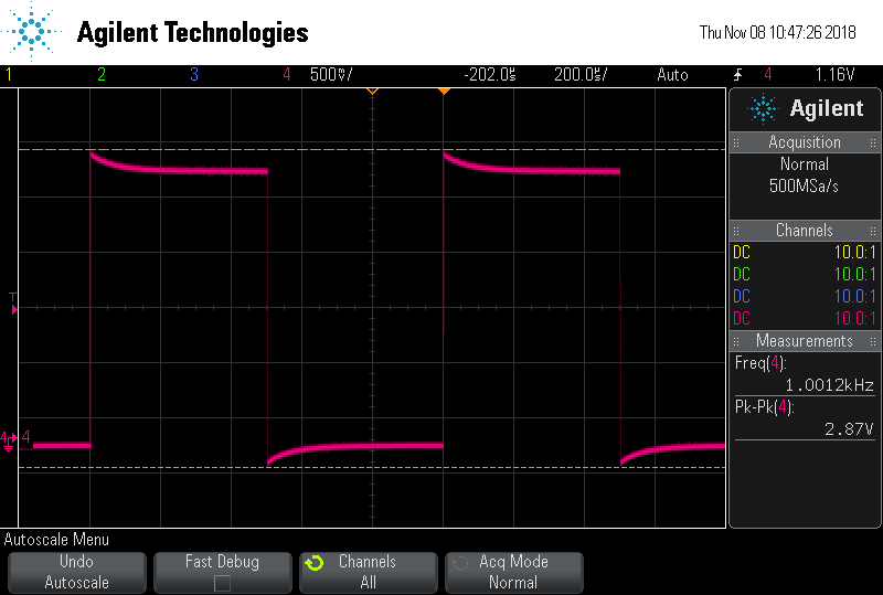
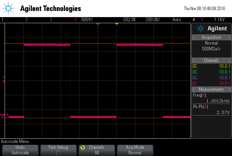
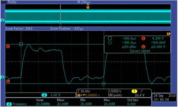
I'm working with a customer who is observing quite a bit of overshoot on the input from their main oscillator.  I'm wanting to know if this is normal, or if we have any techniques we can recommend to reduce it.  Does this violate the operating specifications for the device?

Thanks,

Stuart

  • Hi Stuart,

    What happens when you scope just the output of the oscillator itself without the device connected, do you still see the overshoot?
  • Hi Stuart,

    Can you reply to the previous query?

    Or if the issue is resolved, kindly let us know.
  • Hi Frank:

    I had used the same scope to test two CLK inout signals to the same ground in the same PCBA,  one goes into FPGA,and the other goes to Defino, the difference is a series  27.4ohm have been added line near pin3 of Y2 for FPGA, which is suggest by SI engineer,gererally , this res can be used to reduce the overshoot value, because the distance is shorter between clk chip and Defino than  between CLK chip and FPGA, so we don't add this res there, but the overshoot have exceed 4V for 3.3V logic level of defino IO,not sure whether it is acceptable or not ,we don't find the reference about ovweshoot and undershoot define in the spec, so could you give th refernece for this value, and estimate the risk for chips itsef ,whether are there any other impact for life time or others? you don't need concern the equipment(I ahve checked tha that is ok,theres is no overshoot valur like that), and if overshoot value above 4V is not accetable from your side, I will add the same 27.4 ohm res series between the pin3 and Defino, taht should improve  not only the overshoot but also the undershoot.

    the overshoot test capture for FPGA inp CLK  in the same pcba to the same ground, taht is about 3.8V  

    Zhuo Wang

    Thanks

  • Hi Zhuo,

    This looks to me like a case of under-compensated scope probe. Below 2 captures illustrate what i mean. Same signal being monitored on the scope. In first capture, probe is under-compensated and you can see the significant overshoot and undershoot. In the second capture, the probe is perfectly compensated, no overshoot or undershoot.

    However, if you are confident this is not an issue of under-compensated scope probe and that the overshoot and undershoot are real then yes, your signal is violating X1 input levels. Refer to the screen capture below which i pulled from the datasheet. X1 level shouldn't be more than 0.3V above VDDIO or 0.3V below GND.

  • Hi Zhuo,

    Is this resolved? Do you have anymore questions on this?
  • Hi Frank:

    3.6V is the max limited input logic value, my understanding is that Constant input max volatge is 3.6V, but overshoot is transient peak when signals occurs at the edge of 1->0 or 0->1,in fact ,the overshoot could exceed the max logic value, and I once checked this with FPGA, because there is the same question for other HSI interface logic level, their engineer give me two tabel for reference, which have neen noted fdifferent defination for overshoot value and the max value of logic in the separate table:he said overshoot can impect the life time, but 4V is ok, but the life time is shorter, so whether defino have a different defination for oershoot, do you have other troubleshoooting for IO/CLK application,whether the case of overshoot >3.6V have found in other company exting boards,  it is diffcult to keep transient peak vaoltage below 3.6V in actural product,

    Thanks

    Zhuo Wang

  • Zhou,

    Looks like you might have a transmission line termination problem. I'm looking into this a little bit more and will get back to you tomorrow.
  • Zhou,

    You might already know this but i believe what you are seeing is just reflections from impedance mismatches since because of the high frequency, your board trace wire becomes a transmission line. There is a lot of material online that explains this.

    You have to terminate your signal properly. You have to terminate both at the source and destination. Usually though, termination at one end is sufficient. So either do series termination at the source (close to the oscillator) or parallel termination at the destination (close to the device). I think you were on the right path in your prior post but you were maybe doing the series termination at the wrong end. You might have to calculate out the characteristic impedance of your trace to find the termination resistance you need but you can probably just experiment with a range of resistors till you get what you want.

    Please give this a try and let us know how it goes.
  • Hi Zhou,

    Any update on this? Is it resolved now?
  • Hi Zhou,

    It's been a while since we heard from you. I'm going to assume your problem is resolved so will be marking this thread as closed. If that's not the case, kindly reply to this thread or create a new one if this locks out due to inactivity.