This thread has been locked.

If you have a related question, please click the "Ask a related question" button in the top right corner. The newly created question will be automatically linked to this question.

CCS/TMS320F28377D: PWM Deadbands for witching with a Duity cycle of 100% or 0%

Part Number: TMS320F28377D

Tool/software: Code Composer Studio

Hello community

As you know, in some control method such as DTC or some kind of predictive methods, it is needed that an appropriate switching condition remains during every control cycle. for example "1 0 0 " remains in one or more than one control cycle. It means that high side switch of leg "a" should be on for whole of one or more cycle(s). in other words, duty cycle is always 100% or 0%.

It couldn't find a code sample for adjusting the PWM deadbands for this kind of switching. To my knowledge, the deadbands which are introduced in TRM and used in the examples of developed codes, it is needed that the duty cycle remains lower than 100% or higher than 0%.

Does any way to deal with this issue?

Regards 

  • Yes there are ways to achieve 0% db. I will post it for you today.

  • Hello Nima
    Thanks for prompt reply
    I know how to achieve ZERO deadband! I want to know if there is way of using deadband for 100% or 0% duty cycles (CMPA=100%TBPRD or CMPA=0)

    For more clarifying myself, I wan to generate db while the condition of switching is changed for example from "1 0 0 " to "0 0 0". So the conditions of leg "a" switches should be toggled. It is worth noting that this is never happens during 1 period of PWM in my control method! this transition may occur at the end of any PWM period.
    I'm looking forward hearing from you
    regards

  • Just to clarify your question is,

    Can I use deadband, if I switch between 100% duty cycle and 0% duty cycle? 

    You want a deadband between fully on and fully off?

    Nima

  • Yes Nima, That is exactly what I want.
    Thank you
    regards
  • This is interesting. I have never actually done this before to see if it is possible. I am going to try this on my controlCard. Do you use driverlib or bitfields? just in case I send you some code.

  • This type of deadband should exist for some motor drive control methods such as DTC. Otherwise transition from one switching state to another may damage the power switches.
    I don't know what driverlib is ! I use CCS 6 for coding my Delfino TMS320F28377d.
    regards

  • I will work on a simple code in bitfields,

    the code will look like EPwm1Regs.TBCTR = 0 using bitfield.
    the code will look like Epwm_setCounter(0) using driverlib.

    Not important. I will use bitfields which is most likely what your code uses.

    Nima
  • Thanks a lot
    According to your definition, Yes I'm using bitfield.
    regards
  • Hello Nima
    Still no sound of you!
    Do you think it is impossible or way too complicated?
    regards
  • Sorry about the delay, I was working on 2 other issues. I will work on your as soon as possible.

    Nima
  • Okay, I have a minimum example that hopefully covers the need you have in your system

    The code switches between 100% duty and 0% duty in a loop with a delay.

        for(;;)
        {
            F28x_usDelay(400);
            EPwm1Regs.CMPA.bit.CMPA = 4000;
            F28x_usDelay(400);
            EPwm1Regs.CMPA.bit.CMPA = 0;
            asm ("          NOP");
        }

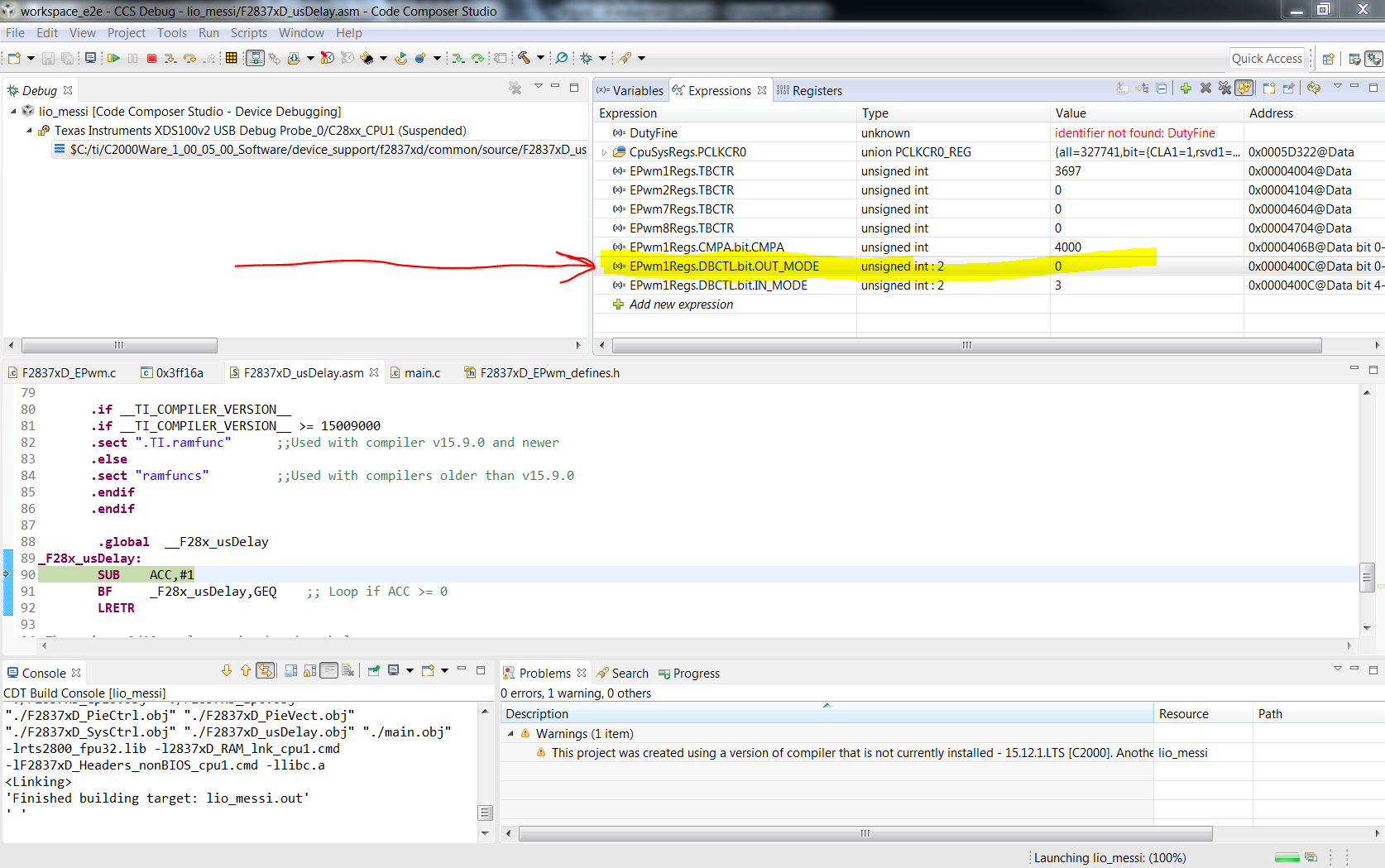
    The deadband module is enabled and initialized with a large enough number. Then inside you Code Composer Studio, you need to add the EPwm1Regs.DBCTL.bit.OUT_MODE bits to be able to switch between enable and disable to see the effects of the deadband module.

    Here is the full code,

    //###########################################################################
    //
    // FILE:    epwm_deadband_c28.c
    //
    // TITLE:   Check PWM Dead-Band
    //
    //! \addtogroup cpu01_example_list
    //! <h1> EPWM dead band control (epwm_deadband)</h1>
    //!
    //! During the test, monitor ePWM1, ePWM2, and/or ePWM3 outputs
    //! on a scope.
    //!
    //! - ePWM1A is on GPIO0
    //! - ePWM1B is on GPIO1
    //! - ePWM2A is on GPIO2
    //! - ePWM2B is on GPIO3
    //! - ePWM3A is on GPIO4
    //! - ePWM3B is on GPIO5
    //!
    //! This example configures ePWM1, ePWM2 and ePWM3 for:
    //! - Count up/down
    //! - Deadband
    //!
    //! 3 Examples are included:
    //! - ePWM1: Active low PWMs
    //! - ePWM2: Active low complementary PWMs
    //! - ePWM3: Active high complementary PWMs
    //!
    //! Each ePWM is configured to interrupt on the 3rd zero event.
    //! When this happens the deadband is modified such that
    //! 0 <= DB <= DB_MAX.  That is, the deadband will move up and
    //! down between 0 and the maximum value.
    //!
    //! View the EPWM1A/B, EPWM2A/B and EPWM3A/B waveforms
    //! via an oscilloscope
    //
    //
    //###########################################################################
    // $TI Release: F2837xD Support Library v3.05.00.00 $
    // $Release Date: Tue Jun 26 03:15:23 CDT 2018 $
    // $Copyright:
    // Copyright (C) 2013-2018 Texas Instruments Incorporated - http://www.ti.com/
    //
    // Redistribution and use in source and binary forms, with or without
    // modification, are permitted provided that the following conditions
    // are met:
    //
    //   Redistributions of source code must retain the above copyright
    //   notice, this list of conditions and the following disclaimer.
    //
    //   Redistributions in binary form must reproduce the above copyright
    //   notice, this list of conditions and the following disclaimer in the
    //   documentation and/or other materials provided with the
    //   distribution.
    //
    //   Neither the name of Texas Instruments Incorporated nor the names of
    //   its contributors may be used to endorse or promote products derived
    //   from this software without specific prior written permission.
    //
    // THIS SOFTWARE IS PROVIDED BY THE COPYRIGHT HOLDERS AND CONTRIBUTORS
    // "AS IS" AND ANY EXPRESS OR IMPLIED WARRANTIES, INCLUDING, BUT NOT
    // LIMITED TO, THE IMPLIED WARRANTIES OF MERCHANTABILITY AND FITNESS FOR
    // A PARTICULAR PURPOSE ARE DISCLAIMED. IN NO EVENT SHALL THE COPYRIGHT
    // OWNER OR CONTRIBUTORS BE LIABLE FOR ANY DIRECT, INDIRECT, INCIDENTAL,
    // SPECIAL, EXEMPLARY, OR CONSEQUENTIAL DAMAGES (INCLUDING, BUT NOT
    // LIMITED TO, PROCUREMENT OF SUBSTITUTE GOODS OR SERVICES; LOSS OF USE,
    // DATA, OR PROFITS; OR BUSINESS INTERRUPTION) HOWEVER CAUSED AND ON ANY
    // THEORY OF LIABILITY, WHETHER IN CONTRACT, STRICT LIABILITY, OR TORT
    // (INCLUDING NEGLIGENCE OR OTHERWISE) ARISING IN ANY WAY OUT OF THE USE
    // OF THIS SOFTWARE, EVEN IF ADVISED OF THE POSSIBILITY OF SUCH DAMAGE.
    // $
    //###########################################################################
    
    //
    // Included Files
    //
    #include "F28x_Project.h"
    
    
    //
    // Function Prototypes
    //
    void InitEPwm1Example(void);
    __interrupt void epwm1_isr(void);
    //
    // Main
    //
    void main(void)
    {
    //
    // Step 1. Initialize System Control:
    // PLL, WatchDog, enable Peripheral Clocks
    // This example function is found in the F2837xD_SysCtrl.c file.
    //
        InitSysCtrl();
    
    //
    // Step 2. Initialize GPIO:
    // This example function is found in the F2837xD_Gpio.c file and
    // illustrates how to set the GPIO to its default state.
    //
    //    InitGpio();
    
    //
    // enable PWM1, PWM2 and PWM3
    //
        CpuSysRegs.PCLKCR2.bit.EPWM1=1;
    
    //
    // For this case just init GPIO pins for ePWM1, ePWM2, ePWM3
    // These functions are in the F2837xD_EPwm.c file
    //
        InitEPwm1Gpio();
    
    //
    // Step 3. Clear all interrupts and initialize PIE vector table:
    // Disable CPU interrupts
    //
        DINT;
    
    //
    // Initialize the PIE control registers to their default state.
    // The default state is all PIE interrupts disabled and flags
    // are cleared.
    // This function is found in the F2837xD_PieCtrl.c file.
    //
        InitPieCtrl();
    
    //
    // Disable CPU interrupts and clear all CPU interrupt flags:
    //
        IER = 0x0000;
        IFR = 0x0000;
    
    //
    // Initialize the PIE vector table with pointers to the shell Interrupt
    // Service Routines (ISR).
    // This will populate the entire table, even if the interrupt
    // is not used in this example.  This is useful for debug purposes.
    // The shell ISR routines are found in F2837xD_DefaultIsr.c.
    // This function is found in F2837xD_PieVect.c.
    //
        InitPieVectTable();
    
    //
    // Interrupts that are used in this example are re-mapped to
    // ISR functions found within this file.
    //
        EALLOW; // This is needed to write to EALLOW protected registers
        PieVectTable.EPWM1_INT = &epwm1_isr;
        EDIS;   // This is needed to disable write to EALLOW protected registers
    
    //
    // Step 4. Initialize the Device Peripherals:
    //
        EALLOW;
        CpuSysRegs.PCLKCR0.bit.TBCLKSYNC =0;
        EDIS;
    
        InitEPwm1Example();
    
        EALLOW;
        CpuSysRegs.PCLKCR0.bit.TBCLKSYNC =1;
        EDIS;
    
    
    //
    // Enable CPU INT3 which is connected to EPWM1-3 INT:
    //
        IER |= M_INT3;
    
    //
    // Enable EPWM INTn in the PIE: Group 3 interrupt 1-3
    //
        PieCtrlRegs.PIEIER3.bit.INTx1 = 1;
    
    //
    // Enable global Interrupts and higher priority real-time debug events:
    //
        EINT;  // Enable Global interrupt INTM
        ERTM;  // Enable Global realtime interrupt DBGM
    
    //
    // Step 6. IDLE loop. Just sit and loop forever (optional):
    //
        for(;;)
        {
            F28x_usDelay(400);
            EPwm1Regs.CMPA.bit.CMPA = 4000;
            F28x_usDelay(400);
            EPwm1Regs.CMPA.bit.CMPA = 0;
            asm ("          NOP");
        }
    }
    
    //
    // epwm1_isr - EPWM1 ISR
    //
    __interrupt void epwm1_isr(void)
    {
    
        //
        // Clear INT flag for this timer
        //
        EPwm1Regs.ETCLR.bit.INT = 1;
    
        //
        // Acknowledge this interrupt to receive more interrupts from group 3
        //
        PieCtrlRegs.PIEACK.all = PIEACK_GROUP3;
    }
    
    
    //
    // InitEPwm1Example - Initialize EPWM1 configuration
    //
    void InitEPwm1Example()
    {
        EPwm1Regs.TBPRD = 4000;                       // Set timer period
        EPwm1Regs.TBPHS.bit.TBPHS = 0x0000;           // Phase is 0
        EPwm1Regs.TBCTR = 0x0000;                     // Clear counter
    
        //
        // Setup TBCLK
        //
        EPwm1Regs.TBCTL.bit.CTRMODE = TB_COUNT_UPDOWN; // Count up
        EPwm1Regs.TBCTL.bit.PHSEN = TB_DISABLE;        // Disable phase loading
        EPwm1Regs.TBCTL.bit.HSPCLKDIV = TB_DIV4;       // Clock ratio to SYSCLKOUT
        EPwm1Regs.TBCTL.bit.CLKDIV = TB_DIV4;
    
        EPwm1Regs.CMPCTL.bit.SHDWAMODE = CC_SHADOW;    // Load registers every ZERO
        EPwm1Regs.CMPCTL.bit.SHDWBMODE = CC_SHADOW;
        EPwm1Regs.CMPCTL.bit.LOADAMODE = CC_CTR_ZERO;
        EPwm1Regs.CMPCTL.bit.LOADBMODE = CC_CTR_ZERO;
    
        //
        // Setup compare
        //
        EPwm1Regs.CMPA.bit.CMPA = 4000;
    
        //
        // Set actions
        //
        EPwm1Regs.AQCTLA.bit.CAU = AQ_SET;            // Set PWM1A on Zero
        EPwm1Regs.AQCTLA.bit.CAD = AQ_CLEAR;
    
        EPwm1Regs.AQCTLB.bit.CAU = AQ_SET;          // Set PWM1A on Zero
        EPwm1Regs.AQCTLB.bit.CAD = AQ_CLEAR;
    
        //
        // Active Low PWMs - Setup Deadband
        //
        EPwm1Regs.DBCTL.bit.OUT_MODE = DB_FULL_ENABLE;
        EPwm1Regs.DBCTL.bit.POLSEL = DB_ACTV_LO;
        EPwm1Regs.DBCTL.bit.IN_MODE = DBA_ALL;
        EPwm1Regs.DBRED.bit.DBRED = 0x3F0;
        EPwm1Regs.DBFED.bit.DBFED = 0x3F0;
    
        //
        // Interrupt where we will change the Deadband
        //
        EPwm1Regs.ETSEL.bit.INTSEL = ET_CTR_ZERO;    // Select INT on Zero event
        EPwm1Regs.ETSEL.bit.INTEN = 1;               // Enable INT
        EPwm1Regs.ETPS.bit.INTPRD = ET_3RD;          // Generate INT on 3rd event
    }
    
    
    //
    // End of file
    //
    

    Okay so here is how to test and verify this,

    load and run the code. Then add the following register to watch window,

    Set the register to 0. Make sure the write takes effect by doing a single step and verifying the new value.

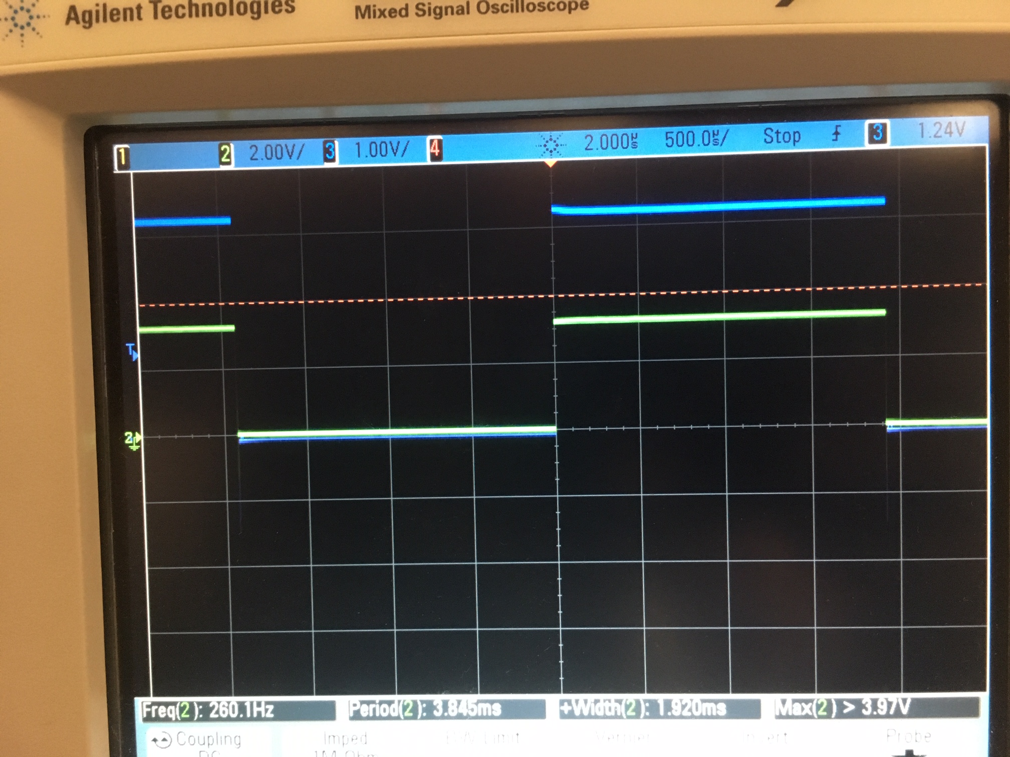
    Run.  The following screen shot from the scope show the DB disabled. As you can see, the OUTPUT A and OUTPUT B of ePWM1 are the exact same. No deadband.

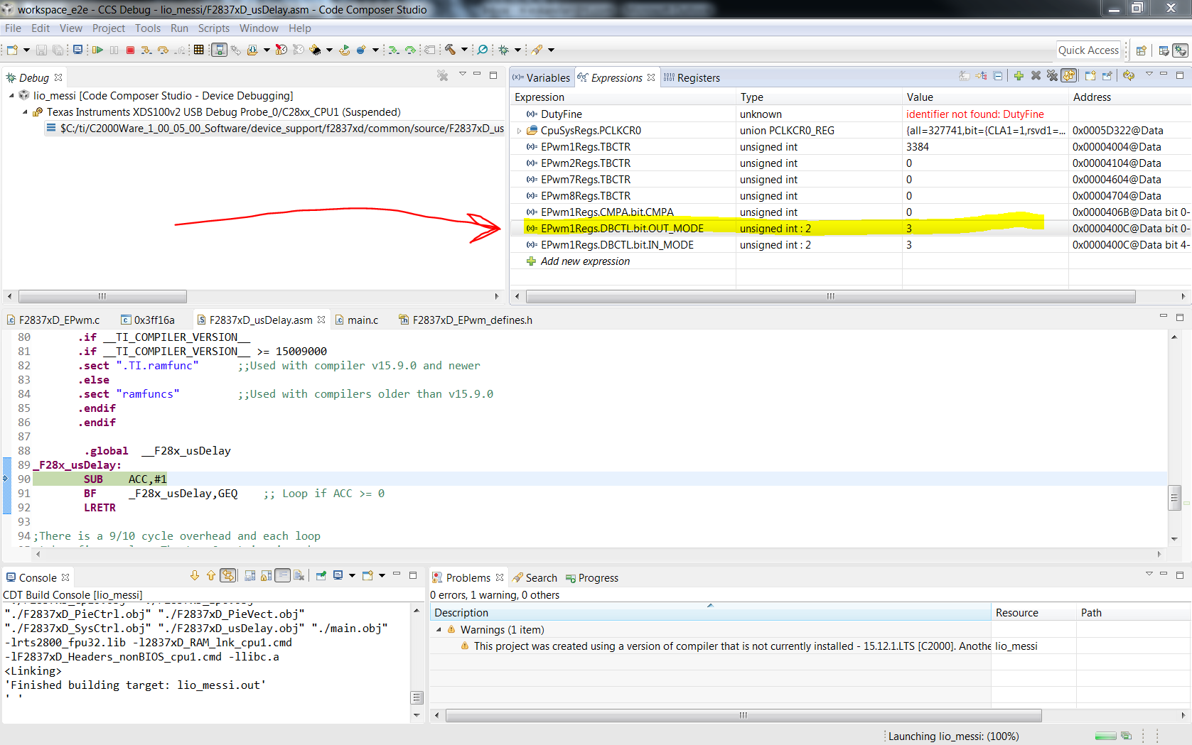
    Halt, change the value to 3.

    Now on the scope you will see that the DB has taken effect and delays have been added.

  • Hello Nima
    Thank you very much for your thorough response.
    But as I see in your code and results, you have taken the duty cycle f the PWM = 50% (i.e., CMPA =4000 for an updown PWM with PRD=4000)
    My question was is it possible to apply the deadbands for 100% duty cycles?
    let me explain with an example:
    consider this switching sequence for EPWM1 : 1-1-1-0-1
    this is 5 sequence of switching in which in first three switching periods, EPWM1A output is high (100% duty cycle) and EPWM1B is low (0% duty cycle). at the 4th switching period, they are toggled (EPWM1A & EPWM1B). after that at the 5th period, again they are toggled.
    considering that in all periods the duty cycle is equal to 100% or 0%, is it possible to use deadbands? in case of a power inverter in this example only between 3rd and 4th periods and 4th and 5th periods the deadband is needed. not between 1st and 2nd or 2nd and 3rd periods.
    Is it possible using our DSP?
    regards
  • That is the PWM going from 100% to 0%. I change the PWM every x amount of US in the main loop from 0% to 100% and back.