This thread has been locked.

If you have a related question, please click the "Ask a related question" button in the top right corner. The newly created question will be automatically linked to this question.

CCS/TMS320F28032: A question about the comparator of 28032

Part Number: TMS320F28032

Tool/software: Code Composer Studio

Hi, I'm Erwin, 

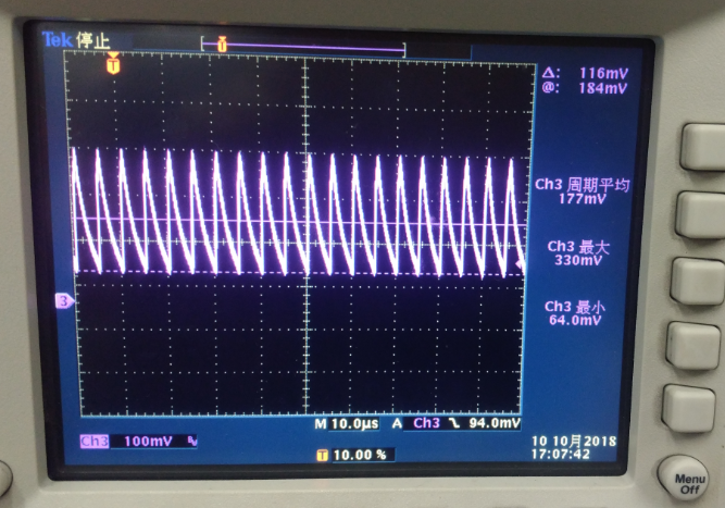
when we are using 28032(LQFP package), we found a strange waveform as below:

Configure COMP2A(14pin) and COMP3A(12pin) as the noninverting terminal of COMP2 and COMP3, internal DAC is connected to inverting terminal of COMP.

when ADC sample function of COMP2B(27pin) and COMP3B(29pin) were enabled, a strange waveform would happen in COMP2A(14pin) and COMP3A(12pin), as the picture showen, the frequency is same with the sample frequency.

if the ADC sample function of COMP2B(27pin) and COMP3B(29pin) were disabled, the phenomenon wouldn't happen.

My question is, why this phenomenon would happen?

Thank you very much

Erwin 
  • Erwin,

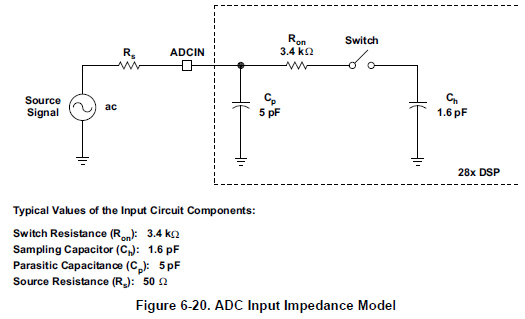
    It is likely that you are seeing the ADC sample and hold capacitor (Ch) charging during the ACQPS window:

    Based on the scope image, I would guess that the source resistance Rs is very high so Ch is not able to charge fully within the ACQPS window.  I recommend either buffering the signal with an op-amp or adding a large capacitor after Rs in parallel with Cp.

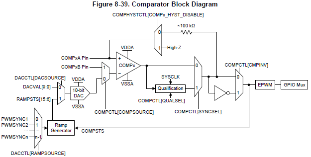
    A large value of Rs will also have problems with the comparator functionality when hysteresis is enabled.  From the F2806x TRM (with the same comparator implementation as F2803x), you can see that there is a ~100kΩ hysteresis feedback signal from the comparator output that will interact with the input source signal:

    -Tommy

  • hi, Tommy,

    Thanks for your reply.

    I have double check with my customer, actually COMPxB is not connected to the negative terminal directly, as the figure shown, the DAC was connected to the negative terminal of the comparator. when my customer doing test, the CompxB was connected to ground, Maybe there is small relationship with Rs.

    Could you help us again to analysis this?

    Thank you

    Erwin

     ,

  • Erwin,

    No, I did not mean to say that the COMPxB has any relationship with Rs.  My point was that the comparator output is fed back to the COMPxA pin through a hysteresis resistor, which can affect the COMPxA pin voltage if the COMPxA source signal has a large Rs.

    The scope picture would make sense if:

    1. The DAC is at a level that is close to tripping the comparator prior to sampling, and
    2. The ADC sampling on COMPxB (ground) injects noise into the device such that the comparator trips, and
    3. Rs is in the kΩ range, which would allow the hysteresis feedback to affect the COMPxA signal

    -Tommy